555 Timer IC Working, Pin Diagram, Examples (Astable, Monostable, Bistable)
Table of Contents
555 Timer IC Introduction:
The 555 Timer IC is one of my favorite ICs. I have been using this timer IC for years in different electronics based projects, for generating pulses, delays, security systems, automation projects, etc. You have no idea the things you can make with this small low-cost Timer IC. This article is fully dedicated to the 555 Timer IC, and I will try my level best to explain the maximum things and share with you some practical examples. But, before I am going to explain different types of circuits that you can build with the 555 Timer IC, first, let’s start with the very basics of the 555 Timer IC.

The 555 Timer IC is an integrated chip used in a variety of timer, pulse generation, and oscillator applications. The 555 Timer IC is used to provide time delays, as an oscillator, and as a flip-flop element. Two other packages of the Timer ICs are available which are 556 and 558. The 556 Timer IC has 2 timing circuits “Dual Timer”, while the 558 Timer IC has a total of 4 timing circuits “Quad Timer”.
The 555 Timer IC was invented by Hans Camenzind and was first introduced in 1972 by Signetics. The NE555 Timer IC is still used throughout the world due to its low price, easy use, and amazing stability. Due to its high demand, the 555 timer ICs are now manufactured in many countries. Alone in 2003, it was estimated that 1 billion units were manufactured. Seriously, the 555 Timer is the most popular integrated circuit ever manufactured.
Amazon Purchase links:
LDR “light dependent resistor”:
Other Tools and Components:
Super Starter kit for Beginners
PCB small portable drill machines
*Please Note: These are affiliate links. I may make a commission if you buy the components through these links. I would appreciate your support in this way!
Why is it Called 555?
This is one of the most commonly asked questions. It is called 555 because of its internal circuit. There are three 5k ohm resistors in the IC which are connected in series between the VCC and GND pins and are used as the voltage dividers. As you can see in the picture below.

Why we need the 555 Timer IC?
It is very simple to generate delays using the Arduino Uno, Arduino Mega, Arduino Nano, PIC microcontroller, etc. But there are situations when we prefer the 555 Timer IC and this is because, the 555 Timer is cheap, easy to use, durable, no programming is needed, and so many other factors. Let me give you an example.
Let’s say you want to make an Automatic Street Lights control system using Arduino. Now, you can do this project using the Arduino Uno or any other controller board. You can easily interface the LDR and a relay module with the Arduino. But you know it will increase the overall project cost. Nobody is going to purchase such a costly circuit. On the other hand, the same project can be done using the 555 Timer IC. Later in this tutorial, I will explain how to make your own Automatic Street lights control system using LDR and 555 Timer IC.
Using the 555 Timer you can make a low-cost motor speed controller, You can make security systems, clap detection system, and so on.
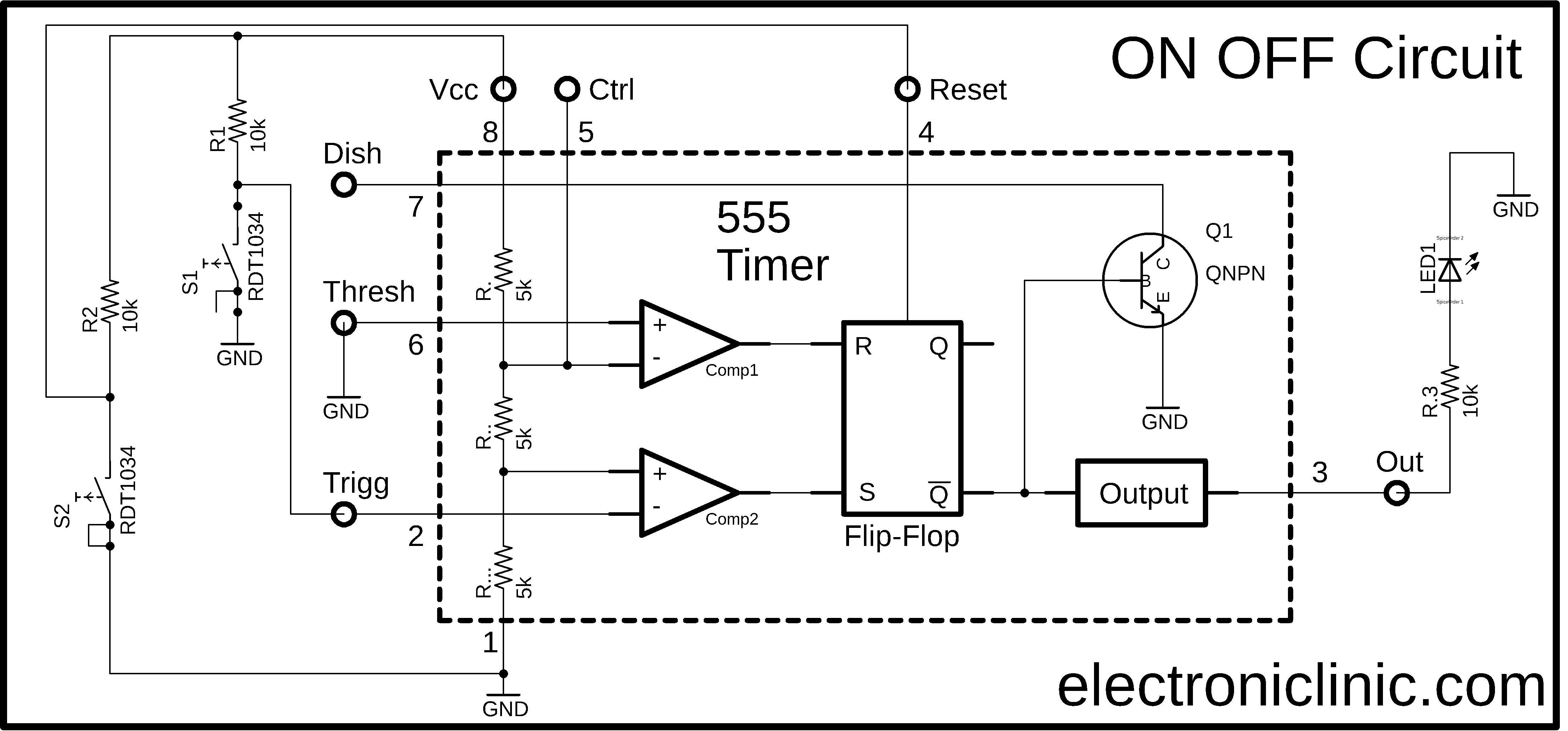
Inside the 555 Timer IC:
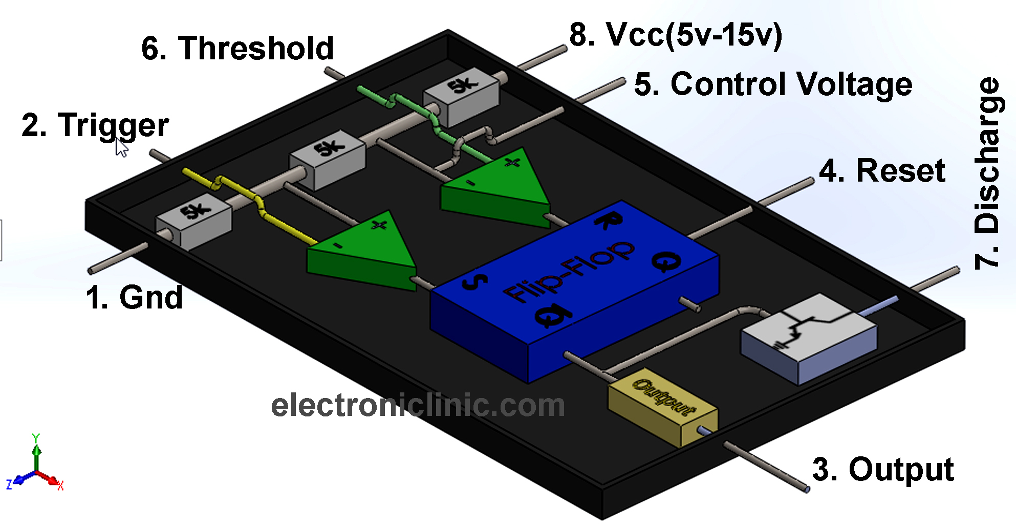
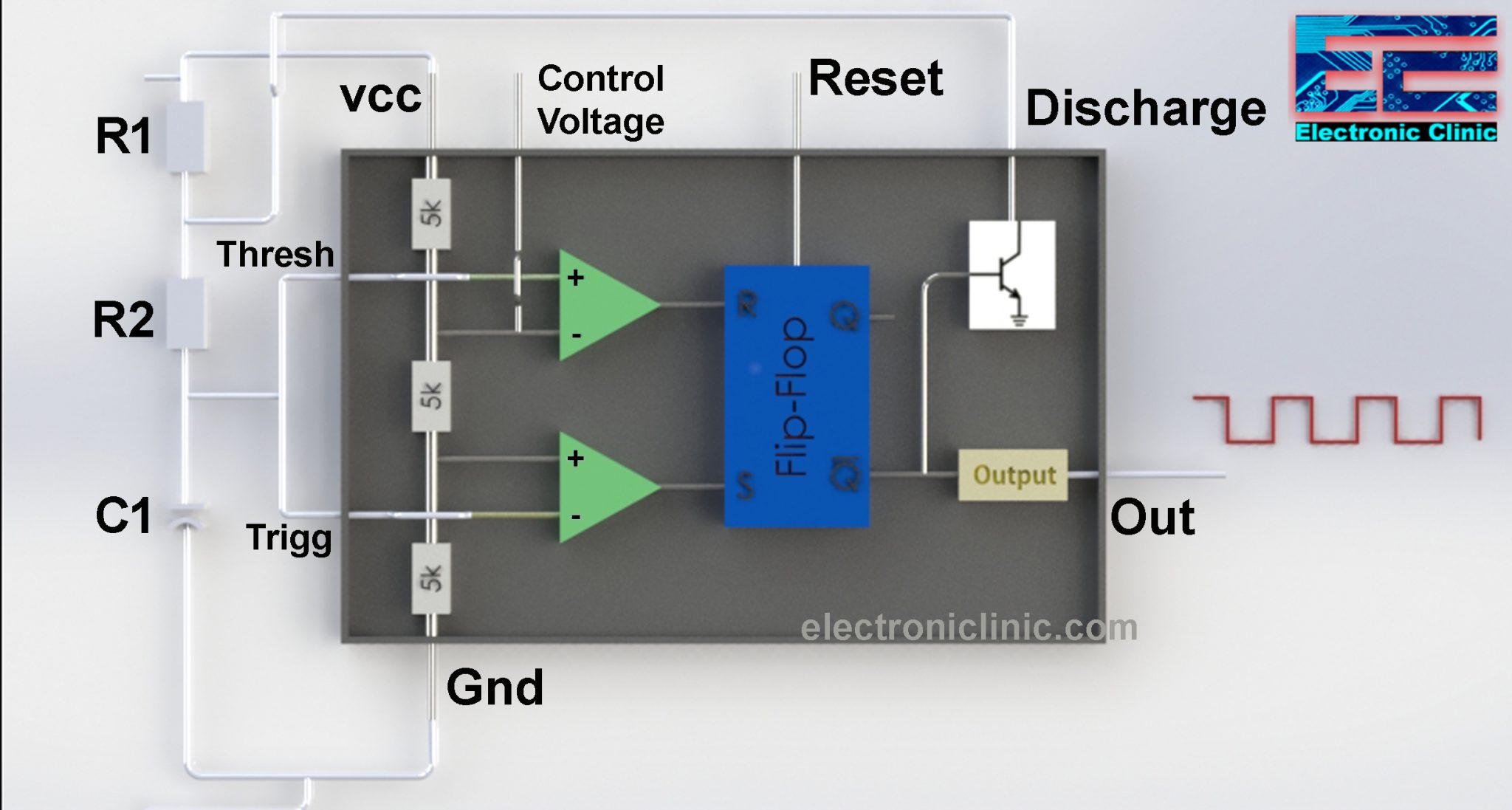
This is the more simplified inside diagram of the 555 Timer IC. As you can see clearly three 5k ohm resistors are connected between the Vcc “Pin 8” and Gnd “pin 1”. This makes the voltage divider circuit, which creates two reference voltages 1/3 and 2/3 of the Vcc “Applied Voltage”.

It has two voltage comparators marked with + and -. + is the non-inverting input while the – is the inverting input. A voltage comparator is an electronic device that is used to compare voltages. The output of the voltage comparator depends on the voltage available at the inverting and non-inverting inputs. If the voltage available at the non-inverting input is greater than the voltage available at the inverting input then the output of the voltage comparator will be high and vice versa.
The two reference voltage 2/3 and 1/3 are connected with the inverting and non-inverting inputs of the two comparators. The inverting input of the first comparator is also connected with the Control Voltage pin. While the non-inverting input of the first comparator is connected with the Threshold and the inverting input of the 2nd comparator is connected with the Trigger pin.
Now the output of these two comparators can be controlled using the Trigger, Threshold, and Control voltage pins of the 555 timer IC. Finally, the result of the comparison of the two comparators which is in the form of 1 or 0 is fed to the Flip-Flop. The output of the first comparator is connected with the R pin of the Flip-Flop while the output of the 2nd comparator is connected with the S pin of the Flip-Flop.
The output of the Flip-Flop is 1 when
R = 0 and S = 1
The output of the Flip-Flop is 0 when
R = 1 and S = 0
The Output Q-bar is connected with the base of the NPN transistor and also with the output stage which has the inverter, which converts 1 into 0 and 0 into 1. So if the output of the Flip-Flop is 1 then the output of the 555 timer IC will be Low, and if the output of the Flip-Flop is 0 then the output of the 555 timer IC will be HIGH.
Moreover, you can reset the Flip-Flop using the 555 timers IC external pin Reset which reset the entire timer.

The output of the voltage comparator 1 is high because the voltage available at the non-inverting input is greater than the voltage available at the inverting input which is 6 volts. Similarly, the output of the voltage comparator 2 is low as the voltage available at the non-inverting input is less than the voltage available at the inverting input. The Flip-Flop converts 0 into 1 which turns ON the transistor which connects the discharge pin of the 555 Timer IC with the ground. The output of the IC 555 Timer will be 0. Now let’s have a look at the pins of the 555 IC and explain each pin in detail.
IC 555 Pin Diagram / Description / configuration / Pinout:

A standard 555 Timer IC package includes 25 transistors, 15 resistors, and 2 diodes on a Silicon chip installed in an 8-pin mini DIP ”dual-in-line package”. Two other packages of the Timer ICs are available which are 556 and 558. The 556 Timer IC has 2 timing circuits “Dual Timer”, while the 558 Timer IC has a total of 4 timing circuits “Quad Timer”. But in this article, we will only discuss the IC 555 timer. As you can see in the picture above, the 555 Timer IC has a total of 8 pins which are clearly labeled as GND, TRIG, OUT, RESET, CTRL, THR, DIS, and Vcc. Let’s talk about each pin in detail.
555 Timer IC Pins description:
- GND “Ground”:
The ground reference voltage, low-level 0V.
- TRIG “Trigger”:
The OUT pin 3 goes high and a timing interval starts when this input falls below ½ of CTRL voltage which is typically 1/3 Vcc, CTRL being 2/3 Vcc by default if CTRL is left open. In other words, the OUT pin remains high as long as the trigger is low. The output of the IC 555 timer totally depends on the amplitude of the external trigger voltage applied to this pin.
- OUT:
This output is driven to approximately 1.7V below +Vcc, or to GND.
- RESET:
A timing interval may be reset by driving this input to GND, but the timing does not begin again until the RESET pin of the NE555 Timer IC rises above approximately 0.7 volts. Overrides TRIG which overrides threshold.
- CTRL “Control”:
Provides control access to the internal voltage divider (by default, 2/3 Vcc).
- THR “Threshold”:
The timing (OUT high) interval ends when the voltage at the threshold pin is greater than that at the CTRL pin (2/3 Vcc if CTRL is open).
- DIS “Discharge”:
Open Collector output which may discharge a capacitor between intervals. In phase with the output.
- Vcc:
Positive supply voltage, which is usually between 3 and 15 volts.
555 Timer IC Features:
- High Current Drive Capability (200mA)
- Adjustable Duty Cycle
- Temperature Stability of 0.005%/ °C
- Timing From µSec to Hours
- Turn off Time Less Than 2 µSec
555 Timer IC Applications
- Precision Timing
- Pulse Generation
- Time Delay Generation
- Sequential Timing
555 Timer IC Working:
The 555 Timer has three modes of Operation which are
- Monostable
- Astable
- Bistable Mode
Let’s talk about each one in detail, before I share with you different 555 Timer-based projects.
555 Timer IC Monostable Mode:
Now, I am going to explain how the 555 Timer IC works in the Monostable mode.

This time I added R1, C1, R2, and a switch S1. As you can see R1 is connected in series with a capacitor C1, this is an electrolyte capacitor. The positive leg of the capacitor is connected with the resistor while the Gnd leg of the capacitor is connected with the ground.
The discharge pin and the non-inverting input of the first voltage comparator are connected between the R1 and C1. The Vcc is 15v. One side of the resistor R2 is connected with the Vcc while the other side of the R2 is connected with the Switch S1, while the other side of the S1 is connected with the Ground. A wire from the middle of the R2 and S1 is connected with the inverting input of the 2nd voltage comparator which is the Trigger pin of the 555 timer IC.
When the switch is open R2 keeps the trigger input High by connecting it with the Supply voltage Vcc. Due to this, the voltage on the inverting input will be greater than the voltage available on the non-inverting input which is 1/3 Vcc. So the output of the 2nd voltage comparator will be zero 0 which is given as the input to the Flip-Flop S pin. We get 1 at the Q bar which turns on the Transistor and discharges the capacitor C1. So this way the voltage available at the inverting input of the 1st voltage comparator “2/3 Vcc” is greater than the voltage available on the non-inverting input. Due to this the output of the 1st voltage comparator will also be zero “0”. So, the Output of the 555 Timer IC remains LOW.
To make the output of the 555 Timer IC High we need to press the switch S1 which is a push-button. The time we press the switch S1 the trigger pin is pulled low and the comparator outputs 1 which is given as the input to the Flip-Flop. The Q-bar gives 0 which keeps the transistor off, due to which now the R1 will charge the Capacitor C1, meantime the output of the 555 Timer IC remains High. As the capacitor is charged and the voltage reaches 2/3 Vcc the Output of the 555 timer goes low.
So the ON time of the 555 timer depends on the value of the resistor R1 and capacitor C1. Large value capacitors will take a lot of time to charge. We can calculate the time by using the following formula.
T = 1.1 * C1 * R1.
555 Timer IC Astable Mode:
The 555 Timer IC in the astable mode acts as the Oscillator which is also known as the free-running Multivibrator. In the Astable mode, the output of the IC 555 timer continuously switches between the High and Low states.
This is a basic circuit diagram of the 555 Timer in the Astable mode. The non-inverting and inverting inputs of the two voltage comparators are connected together and then connected with the middle of the R2 and C1. Two resistors R1 and R2 are connected in series with the capacitor C1. A wire from the middle of R1 and R2 is connected with the IC 555 Timer Discharge pin.

Now, let’s see how this works, When we power up the circuit the resistors R1 and R2 will start charging the capacitor C1, you know it takes time to charge. During the charging process, the voltage on the trigger pin of the 555 Timer remains lower than the 1/3vcc, due to which the comparator outputs 1 which is given as the input to the Flip-Flop and the Q-bar gives 0, which keeps the transistor in off state while the output of the 555 timer IC remains High. Now, this output will remain High until the capacitor C1 charges to the point where the voltage available on the Trigger pin gets high than the voltage available on the non-inverting input of the 2nd comparator. The output of the threshold comparator is 0 as the capacitor continues to charge.
Now for low output, let’s say the capacitor C1 is fully charged or charged enough that the voltage at the trigger pin is greater than the 1/3vcc. The output of the 2nd comparator will be 0 and the output of the 1st comparator will be 1. The Q-bar will output 1 which will turn on the transistor and connects the R1 with the ground. The capacitor C1 then discharges through the resistor R2, due to which the voltage reduces and the outputs of the comparators are changed. This keeps the 555 Timer IC output Low.
The same value resistors will give you the same on and off times. Changing the values of R1 and R2 the on-time and off-time can be adjusted. For the variable ON and OFF time use variable resistors. Replace R1 and R2 with variable resistors.
Formuals:
ON-Time:
Ton = .0693 * (R1 + R2) * C1
OFF-Time:
Toff = 0.693 * (R2) * C1
Period for one cycle:
T = Ton + Toff = 0.693 *(R1 + 2R2)C1
Frequency:
F = 1/T
F = 1/(.693 * (R1 + 2R2)C1
F = 1.44/(R1 + 2R2)C1) Hz
555 Timer IC Bistable Mode:
Now, finally, we will see how the 555 Timer IC works in the Bistable Mode.
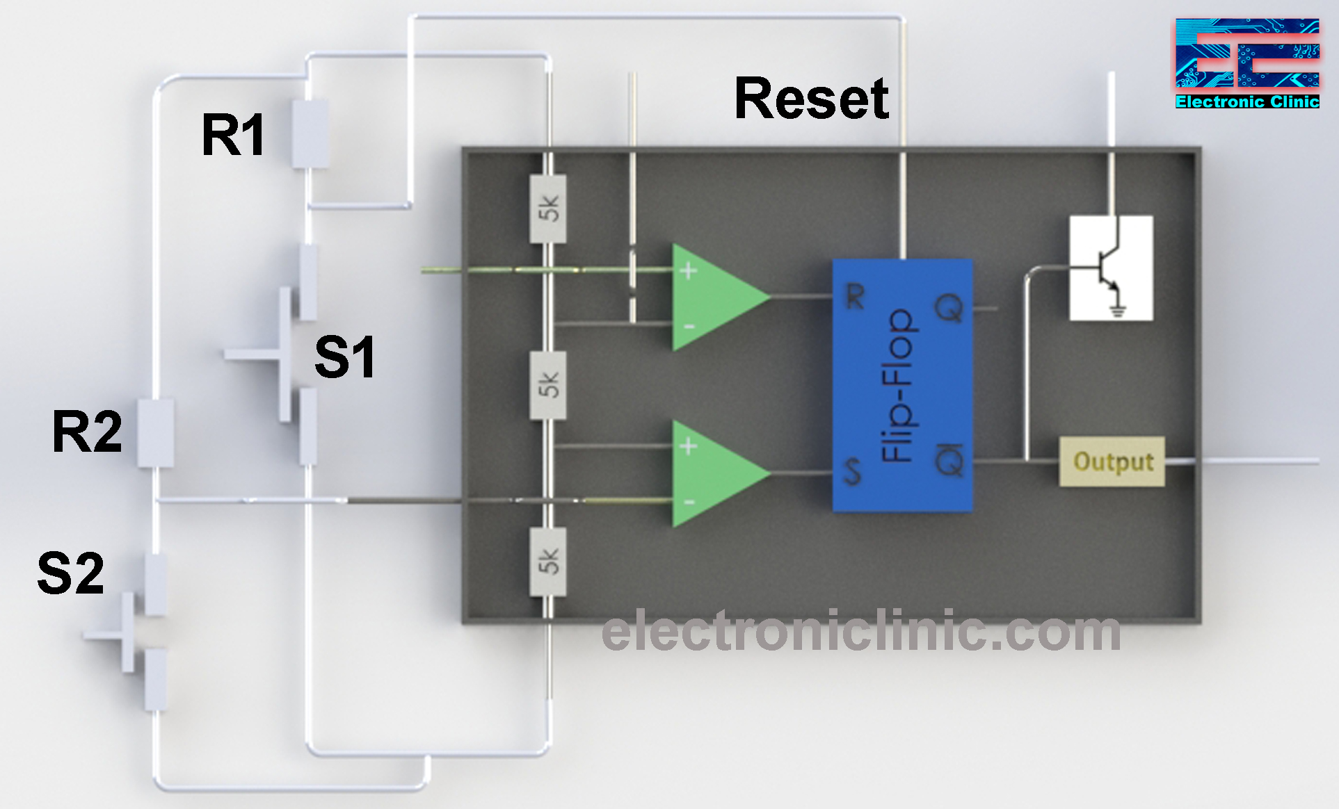
The reset pin is connected with the middle of the R1 and Switch S1. While the switch is open R1 keeps the reset pin at a logic level high. The inverting pin of the 2nd voltage comparator is connected with the R2 and S2, while the S2 is open the trigger pin is kept high by the R2 as it supplies the Vcc to the inverting pin of the voltage comparator. Don’t forget to connect the threshold pin of the 555 Timer IC with the Gnd. Now let’s see how this works.
Let’s consider that no switch is initially pressed, the voltage available at the inverting input of the 2nd comparator is 15v which is greater than the voltage available at the non-inverting input, this comparator outputs 0 which is fed to the S pin of the Flip-Flop and then the Q-bar outputs 1 and the output of the 555 timer is Low. This output will remain Low until we press the switch S2.
Now, let’s consider that the switch S2 is pressed this will pull the inverting input of the comparator to ground due to which the voltage available on the non-inverting input get high than the voltage available on the inverting input, so, the comparator generates 1 at the output which is given as input to the S pin of the Flip-Flop and then the Q-Bar outputs 0 and the timer outputs becomes High “the output stage has the inverter which converts 1 into 0 and 0 into 1”. This output will remain high until we press the switch S1. So, the 555 Timer IC in the Bistable mode acts as the toggle switch. It can be ON or OFF.
So, now after covering the basics, it’s time to make some basic, intermediate, and advanced level projects using the 555 Timer IC.
555 Timer IC-based Projects:
555 Timer Power-ON delay circuit:
The 555 Timer Power-ON delay Circuit can be used in different projects where you need to turn ON a specific load for a certain amount of time. In this project, the 555 Timer IC is used in the Monostable Mode. The purpose of this project is to turn on the load for a few seconds each time the button is pressed or a sensor is activated. This 555 Timer-based delay circuit can also be used in the security systems for turning ON the buzzer for a certain time period which can be calculated using the formula already discussed above. The circuit which I am going to explain can also be used with the PIR, Laser, Push Buttons, etc. This Power-ON delay circuit can be really beneficial in projects where you don’t want to use the expensive controller boards like Arduino, and Mega. Now, let have a look at the circuit diagram.
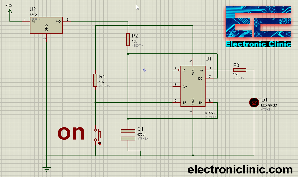
Download the Proteus Model of the 555 Timer-based Power-ON delay circuit by clicking on the Download button given below:
Download: 555 timer power on delay circuit
As you know the Vcc can be up to 16 volts. But I am going to use 12 volts as a 12v adaptor that can be easily arranged. As you can see I have used a 12v regulator LM7812. The output of the 12v regulator is connected with the VCC of the IC 555 Timer and the ground of the regulator is connected with the ground pin of the 555 Timer. The resistor R2 is connected in series with the capacitor C1 which makes the RC circuit. The time delay depends on the R2 and C1. Changing the value of R2 or C1 the time delay can be changed.
The Discharge and Threshold pins of the 555 Timer IC are connected with the middle of R2 and C1. The R1 and a Push Button are connected in series. The other side of the push button is connected with the ground.
For the best understanding, I have connected an LED at the output pin of the 555 Timer IC. Later in other examples, I will explain how you can replace this with a transistor to control high loads.
Working of the Power-ON Delay circuit:

Initially, when you turn ON the circuit, the LED will turn ON, and it will remain ON for a certain amount of time depending on the value of the resistor R2 and the capacitor. As you can see in the circuit above, Vcc is connected with the Trigger pin through a 10k resistor R1, due to which the voltage on the inverting pin of the comparator 2 is greater than the voltage available on the non-inverting input, so the comparator outputs 0, which is given as the input to the S pin of the Flip-Flop. On the Q-bar it outputs 1 which turns ON the transistor which connects the threshold pin with the ground and starts discharging the capacitor, during this time the led remains ON if the capacitor has the charge. When the capacitor voltage drops and the voltage on the non-inverting input of the comparator 1 get low below the voltage available on the inverting input of the comparator1, the comparator 1 will output 0. The LED will turn OFF.
Now to again turn ON the LED, we will need to press the push button, which will connect the inverting pin of the comparator 2 with the ground, due to which the comparator 2 will output 1 which is given as the input to the S pin of the Flip-Flop. The Q-bar give 0 and the output stage gives 1 which turns on the led and also the capacitor starts discharging and the led remains ON until the capacitor is discharged to the point where the voltage available on the Non-inverting input of the comparator 1 gets low below the voltage available on the inverting input.
The LED will remain OFF until we press the push-button again. This is how the 555 Timer-based Power ON delay circuit works.
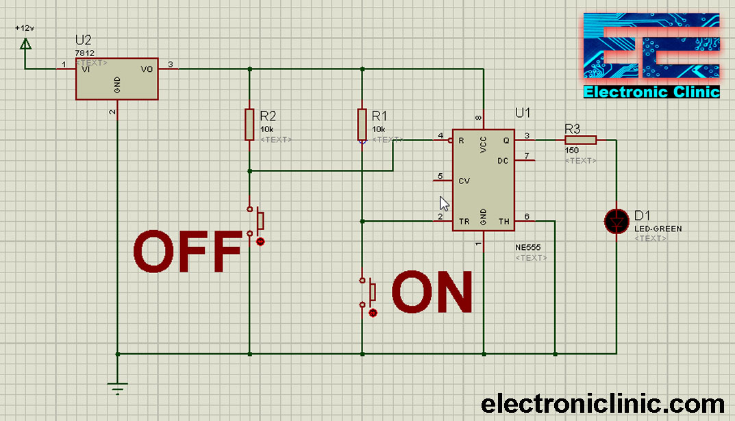
555 Timer ON-OFF Switch Circuit:
The 555 Timer-based ON-OFF circuit is given below. In this small project the 555 timer IC is used in the Bistable mode and following is the same circuit which I have already explained above. I tested this circuit in a Proteus simulation and it worked just fine. The Led connected at the output can be turned ON and turned OFF using two pushbuttons.
Download the Proteus Model of the 555 Timer-based ON-OFF circuit by clicking on the Download button given below:
Download: 555 timer ON OFF swtich toggle switch
The LM7812 regulator is used to power up the 555 timer ic which I have already explained in very detail. The LED connections remain the same. A 10k resistor R1 is connected in series with a Push Button. A wire from the middle is connected with the Trigger pin of the IC 555 Timer. The 12 volts are connected with the Trigger pin through the 10k resistor R1.
Another 10K resistor R2 is connected in series with a Push Button and a wire from the middle is connected with the Reset pin of the 555 Timer. Now we will see how this circuit works.
Initially when the circuit is turned ON Vcc “12 volts” is connected with the Trigger pin of the 555 timer IC through a 10k resistor R1. So the voltage available on the inverting input is greater than the voltage available on the non-inverting input, due to which the comparator 2 outputs 0 which is given as the input to the S pin of the Flip-Flop which converts this into 1 and the output stage converts this into zero so the led remains OFF.
Now if you press the Switch S1 this will connect the trigger pin with the Gnd due to which the voltage available on the non-inverting input gets greater than the voltage available on the inverting input, so the comparator will output high “1”. The Flip-Flop then converts this into 0 and the output stage again converts this into 1 which turns ON the LED. Now, this LED will remain ON until we press the Switch S2 which will reset the 555 timer IC and the LED will turn OFF.
Now to again turn on the LED, you will need to press the switch S1. So this way using two push buttons we can turn ON and turn OFF an LED or any load. The switches can be replaced with sensors for automatic operations.
555 Timer with ON-OFF pulse “Variable duty cycle”:
In this project, the 555 Timer IC is used in the Astable model.

Download the Proteus Model of the 555 Timer based ON OFF pulses by clicking on the Download button given below:
Download: 555 timer on-off pulses
The two variable resistors can be used to vary the ON-Time and OFF-Time. The working of the 555 Timer IC in the Astable mode is already explained in very detail. If you want the perfect square wave of the same duty cycle then use resistors of the same value. The ON-Time and OFF-Time depend on the values of the resistors and capacitor C1.
555 Timer recommended values of Components:
Ra = Rb >= 1K <= 1.5M ohm
The minimum values of the resistors used being 1k is really important, so that 555 Timer IC won’t get damaged due to the excess inflow of current. Its also important not to exceed the maximum value of Ra and Rb to 1M, so that the 555 IC can get enough current required for the leakage current of the electrolytic capacitors. One more thing you can use a maximum value of C = 1000 uf as any bigger capacitors will discharge too much current through the chip, which can damage the 555 Timer IC.
555 Timer Christmas lights Fireflies effect:
Inspired by the Fireflies lighting effect I decided to make something for Christmas. This is an amazing project specially designed for the trees. The lighting effect is just like the Fireflies. You can use multiple of these circuits, set different on and off times, this way you will get a random effect, which will give you a feeling of if so many fireflies are in the tree.
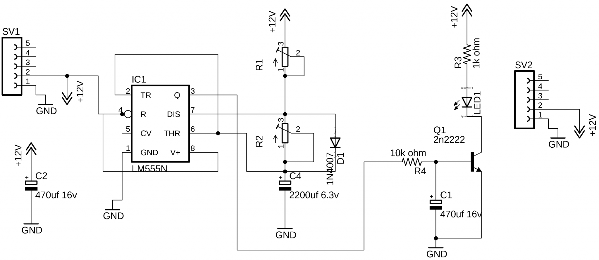
Using this circuit you can vary the duty cycle. For the fading effect, 470uf capacitor is connected at the base of the 2n2222 NPN transistor. The purpose of using this transistor to increase the current handling capability, this way you can use brighter LEDs that need more milliamps. Using the R1 and R2 variable resistors or Potentiometers you can adjust the ON-time and Off-time of the LED.
For the practical demonstration watch video given at the end of this article.

About the PCBWay:
The PCB board used in this project is sponsored by the PCBway Company, which is one of the most experienced PCB and PCB assembly manufacturer. They create high-quality PCBs at reasonable prices. The Gerber files of the PCB board used in this project can be downloaded from the PCBway
Download Gerber Files: “ link will be available soon “
High quality & Only 24 Hours Build time: “https://www.pcbway.com/”
Automatic Street Light using 555 Timer and LDR:
Automatic Street Light using 555 Timer and an LDR- This is seriously an amazing project and no doubt this is one of my favorite projects. This is a very small project build around a few electronic components. In this project, you will learn how to make an automatic street light control system using 555 timer IC and an LDR. You can also use this circuit in lawns. Before, I am going to explain the circuit; first, I would like to explain why we need this circuit in the first place and how this project works.
A lot of electricity is wasted when there is no automatic switching. The lights remain ON in the morning because there is no one to switch off the street lights or lawn lights. This results in increased bills and wastes a lot of electricity.
For such a small project, it’s not practical to use the Arduino board. Such a simple task can be accomplished by using the 555 timer IC. This way, we can keep the project overall cost low.
When the darkness is detected by the LDR, the 555 timer turns on the street lights or lawn lights. The circuit should be placed in the area where the street lights never fall on the LDR. In the morning when the Sunlight falls on the LDR the street lights are automatically turned OFF.

Download the Proteus Model of the 555 Timer-based street lights automatic control system by clicking on the Download button given below:
Download: automatic street lights using 555 timer and ldr
At the output of the 555 timer IC an LED is connected which you can replace with a relay to control higher AC/DC loads. An LDR “light dependent resistor” is connected in series with a 10k variable potentiometer. The advantage of using the variable resistor is that, we can adjust the light sensitivity by rotating the knob of the variable resistor. The LDR and the variable resistor make a voltage divider. A wire from the middle of this voltage divider is connected with the Trigger pin of the 555 Timer IC. The voltage on the Trigger pin varies as the light intensity changes. If you have read the things I explained above at this point you should be able to figure out how the output of the 555 Timer changes as the voltage varies on the Trigger pin of the 555 IC.
The voltage on the trigger pin of the IC “which is the inverting input of the comparator” which is coming from the voltage divider “formed by the LDR and variable resistor” is compared with the voltage available on the non-inverting input of the comparator. So, when the voltage on the inverting input is greater or lower than the voltage on the non-inverting input the output is controlled accordingly, which is an automatic operation.
This is a small low-cost automatic street light controller circuit based on the 555 timer and an LDR. Apart from the street lights, this circuit can be used in areas where you need to control anything on the light basis.
So many other projects can be built using the 555 Timer IC. I will try to add more projects based on the 555 Timer. I hope this article helps you. If you have any suggestions or questions let me know in a comment.
Subscribe to my Website and YouTube channel.
Watch Video:
555 timer datasheet:
https://pdf1.alldatasheet.com/datasheet-pdf/view/53594/FAIRCHILD/NE555.html