Introduction to the 741 OP AMP, Circuit Diagram, and working
Table of Contents
741 OP-AMP Operational Amplifier:
Introduction to the 741 OP AMP, Circuit Diagram, and working- In 1965, the Fairchild semiconductor company introduced the first and most largely used µA709 monolithic operational amplifier. Though this amplifier was very successful, despite this, it had some flaws. A better and more advanced version of µA709 OP-AMP was introduced after removing the loopholes and drawbacks existing in it. It is known as µA741 OP-AMP. Due to its low costs and easy use of µA741, the OP-AMP achieved remarkable achievement. Various manufacturers manufactured different designs of µA741 operational amplifiers e.g. Motorola manufactured MC1741, National Semiconductor LM741, and Texas Instruments SN72741. All these monolithic operational amplifiers are equivalent to µA741 OP-AMP because all of their characteristics and descriptions are the same on the data sheets. For simplicity purposes, the majority of people ignore its initial letters and term this all-famous operational amplifier just as 741.
Number 741 has become an industry standard. Principally, the manufacturing of any kind of new design starts from 741, because it serves as a standard. Therefore, 741 are considered a basic device. 741 OP-AMP operational amplifiers are available in the market in several numbers e.g. 741, 741A, 741C, 741E, and 741N, etc. These amplifiers differ from one another by means of voltage gain, temperature range, noise level, and other characteristics. 741C (C means commercial) is the cheapest and most widely used operational amplifier. Its open-loop voltage gain is 100,000 its input impedance 2MΩ and its output impedance is 75Ω.
Circuit Diagram of 741 OP-AMP
In figure 8.64, a simplified circuit diagram of a 741 OP-AMP operational amplifier has been illustrated. The circuit is equivalent to 741 and many other OP-AMP which was manufactured subsequently. It is not necessary to learn a complete detail about its design, just understanding the working mechanism of the circuit would be enough.
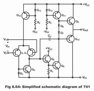
Working Method
The input stage of this circuit consists of a differential amplifier in which two transistors Q1 and Q2 are being used. In this circuit, Q14 transistor is a current source. R2, Q13, and Q14 are the current mirror that generates tail current for Q1 and Q2 (in other words, R2 and Q13 combined together control bias of Q14 which generate tail current or current source for differential amplifier). Instead of using an ordinary resistor as a differential amplifier’s collector resistor, an active load resistor is applied in a 741 OP-AMP. Thus, the voltage gain of a differential amplifier is quite high as compared to a passive load resistor.
Amplified signal achieved through a differential amplifier, operates Q5 base, which is an emitter follower. This stage enhances the impedance level of the differential amplifier. The signal received from Q5 is transmitted on Q6. Diodes Q7 and Q8 are a part of the final stages of biasing. Q11 transistor operates as an active resistor for Q6. Thus, Q6 and Q11 are just like a common emitter (CE) driver stage with an immensely high voltage gain. An amplified signal from the common emitter stage (Q6), moves towards the final stage, which comprises class B push-pull emitter follower (Q10 and Q9). As a result of split supply (equal positive VCC and negative VEE voltages) output becomes zero at that time when the value of input voltage is zero. Any kind of change within zero volts is known as an output error voltage.
When the value of V1 exceeds V2, input voltages Vin produces positive output voltages Vout. When the value of V2 exceeds V1, input voltages Vin produce a negative output voltage Vout. Prior to the occurrence of clipping in case of an ideal situation, Vout can be positive like +VCC and negative just like –VEE. Thus, due to a voltage drop in 741, a variation in output between 1 to 2V occurs in the shape of a voltage supply.
Two examples of active loading are present in the circuit shown in the figure (i.e. transistors have been used on loads in place of resistors). First example is that of the active load (Q4), which has been mounted on input side of the differential amplifier. The other active load is Q11 which exists on common – the emitter driver stage. As the current source has the capacity of high output impedance, therefore active loads produce very high voltage gain as compared to the possible gain expected to be achieved from an ordinary resistor. These active loads generate a definite voltage gain of 100,000 in the case of a 741C OP-AMP. Active loading is extremely popular in integrated circuits because is comparatively easy to manufacture a transistor instead fabricating a resistor on the chip.
Next Topic: Introduction to Comparator
Previous Topic: Applications of Amplifiers, Inverting, Non-inverting
For electronics and programming-related projects visit my YouTube channel.