JFET, Junction Field Effect Transistor, JFET Construction, JFET Operation
Table of Contents
JFET Junction Field Effect Transistor:
JFET:- It is a three-terminal Unipolar Semiconductor device in which current is controlled by electric field. Since, only one type of majority carrier i.e. Electrons or holes are used for the operation of FETs. So FETs are called as Unipolar semiconductor device. FETs are used both in digital and analog circuits. FET are used as switch in digital circuits while it is used as Amplifier (voltage amplifier) in analogue circuits. There are two types of FETs
- Junction field effect T/r JFET
- Metal Oxide semi conductor field effect T/r (MOSFET)
Junction field-effect T/r JFET:
JFET Construction:
It is generally fabricated with either N-channel or P-channel. Hence we can say that JFETs are of two types.
- N-channel JEFT
- P-channel JEFT
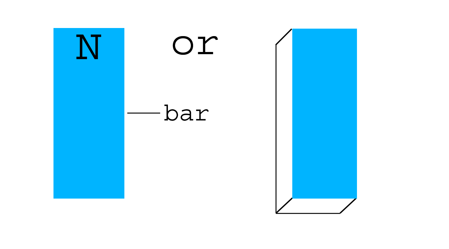
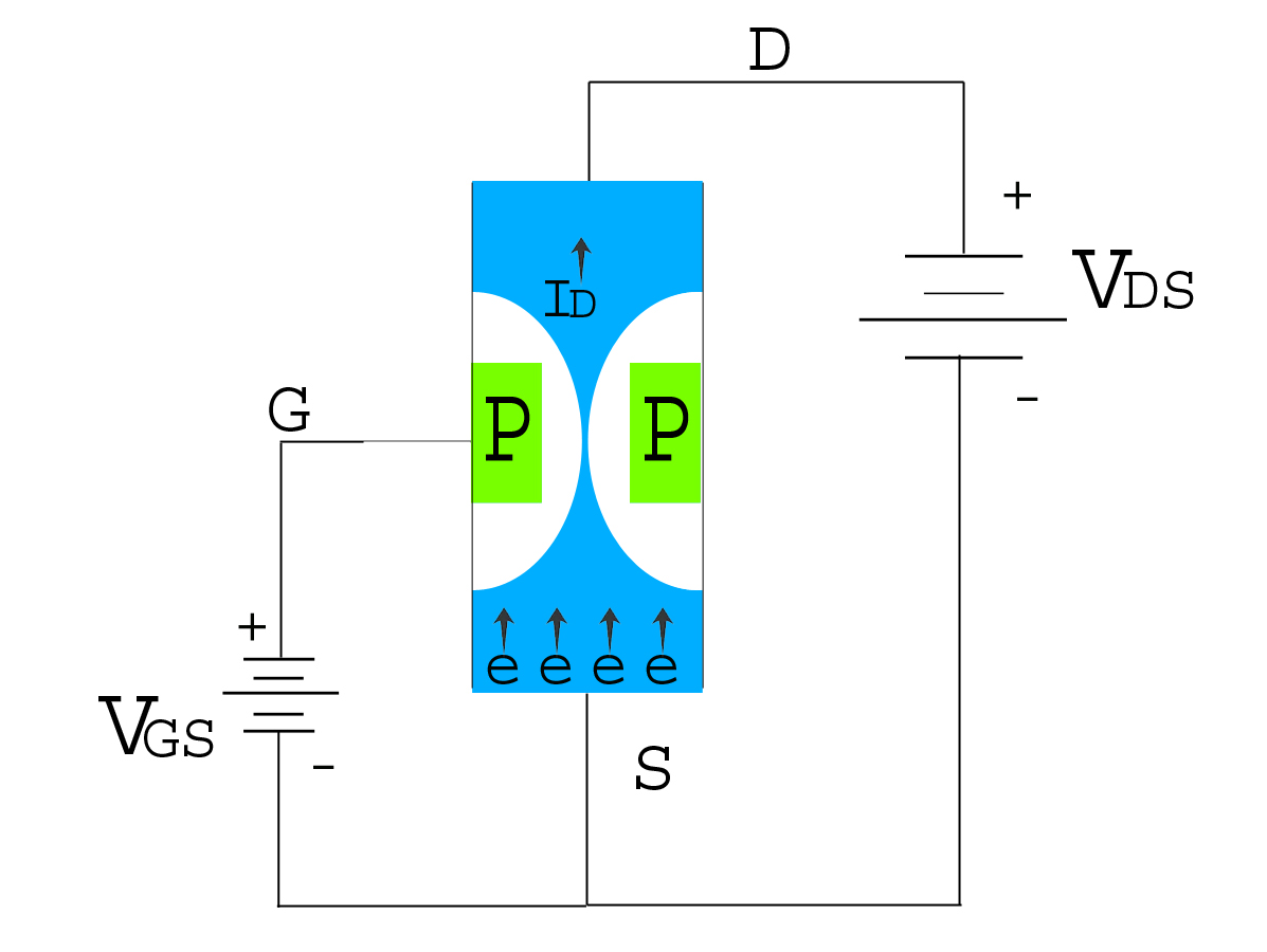
But we will prefer N-channel (for its higher speed of current). For fabricating N-channel JEFT, first of all, a bar of N-type semi-conductor (silicon) is taken as shown below.
Two P-type junctions are diffused on opposite sides of the middle part of the bar shown in figure below.
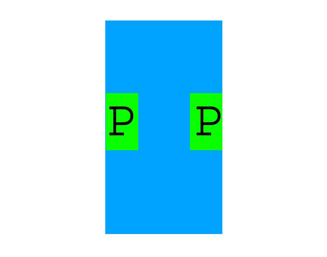
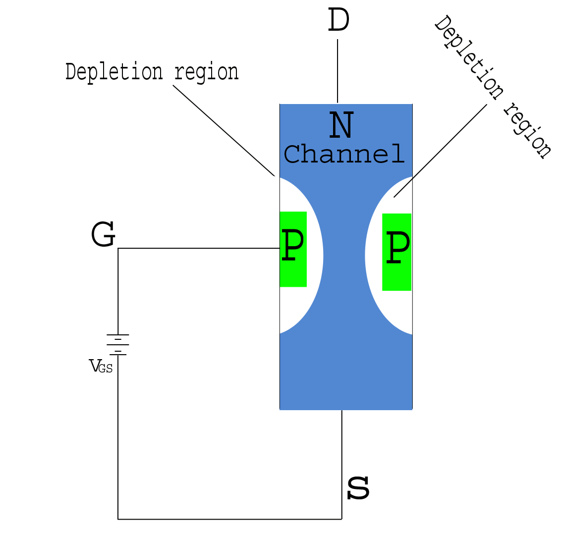
These junctions form two PN-junctions (diode) called gates. The area b/w these gates is called channel. Channel is the conducting path b/w source and drain. The two P-regions are internally connected and a single lead is brought out, which is called gate terminal as shown in the figure given below.
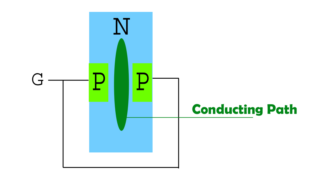
The gate bar is denoted by “G” this bar behaves like a resistance. Ohmic Contacts i.e. direct electrical connections are made at the two ends of the bar. The lower end of the bar having lead is called source terminal and is denoted by “S” upper end of bar having lead is called drain terminal and is denoted by “D”. Now the structure and symbolic representation of N-channel JEFT is given as.
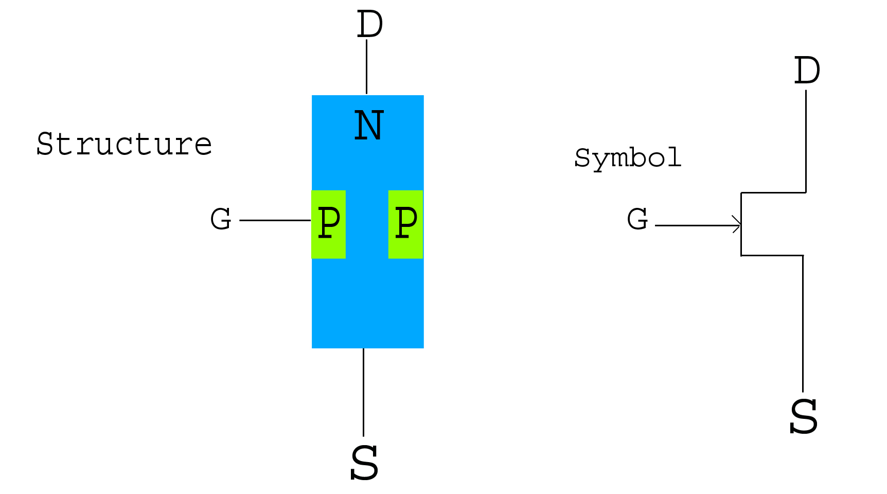
The arrow head is always at gate terminal “G” and for N-type channel arrow is into the gate and for P-type channel the arrow head is out of gate as shown in figure below.
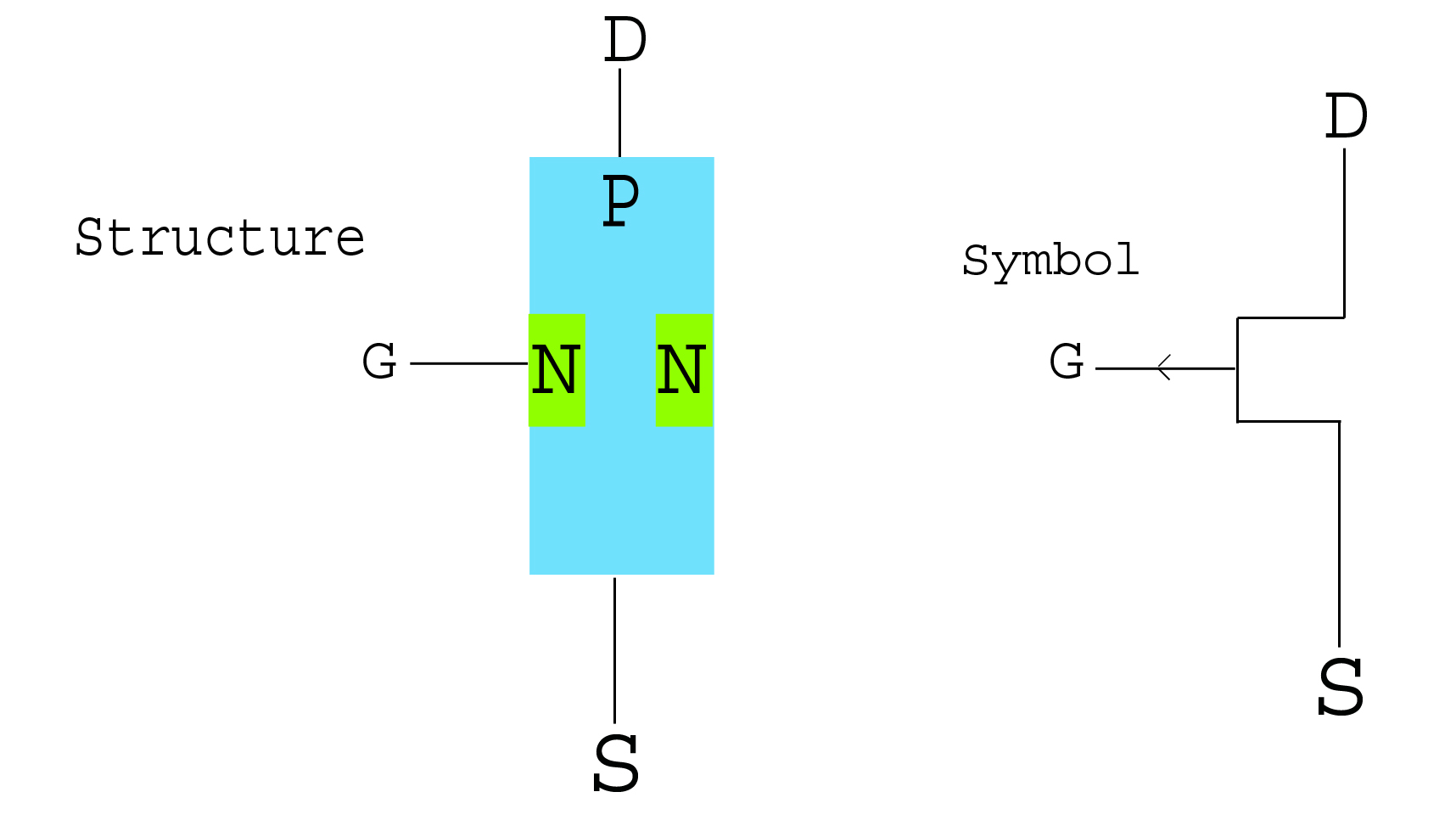
It is a three terminal device namely source, drain, and gate. They are defined as
Source: It is the terminal through which majority carriers enter into the bar towards drain, so it provides majority charge carriers (electrons for N-channel and holes for P-channel). Source resembles with emitter in bi-polar junction T/r.
Drain: It is the terminal through which majority carriers leave the bar. This terminal is similar to collector of bi-polar junction T/r.
Gate: The two P-regions are internally connected and a single terminal is brought out which is called gate terminal, it is a control terminal, it produces electric field. It can change the conductivity of the channel. it is similar to the base of bi-polar junction T/r.
Operation of JFET:
For the proper operation of JFET the gate is always reversed Biased. So the gate current IG is practically zero IG = 0. The Source terminal is always connected to that end of the Drain voltage supply which provides the necessary charge Carriers that are majority charge carriers.
In N-channel JFET the source terminal “S” is connected to the -Ve end of the drain voltage supply (for obtaining electrons which flows through the channel).
In P-channel JFET the source terminal “S” is connected to the +Ve end of the drain voltage supply (for obtaining holes which flows through the channel).
Now let us consider N-channel JFET:
The gate is made up of P-type semiconductor material (holes are in majority).There are two reversed biased P-N junctions. During reversed biased of gate the -Ve end of the voltage source VGS is connected with gate terminal. One P-N junction is shown below.
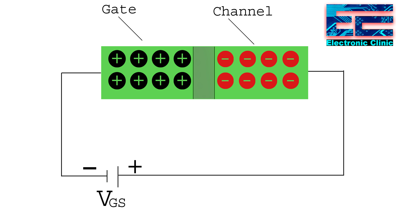
Due to reverse biased the free charges (holes and electrons) move away from the junction, as opposite charges attract each other as shown in figure given below.
A depletion region is developed across the junction. Similarly, another depletion region is developed across the second P-N function. The depletion region is defined as “a region having no charge carrier”. As shown in figure given below.
The depletion region reaches the path for the conduction that is passage for the majority carriers; Area of the channel decreases and resistance of the channel increases (very very small gate current is there) further increase in the -ve voltage, further reduces the channel area and a voltage is reached at which the depletion regions meet each other or touch each other and the channel is completely blocked. The current IG practically become zero IG = 0, due to the reversed bias the input resistance of JFET is very very high (approximately 1000 mega). It is shown in figure below.
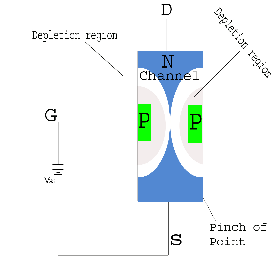
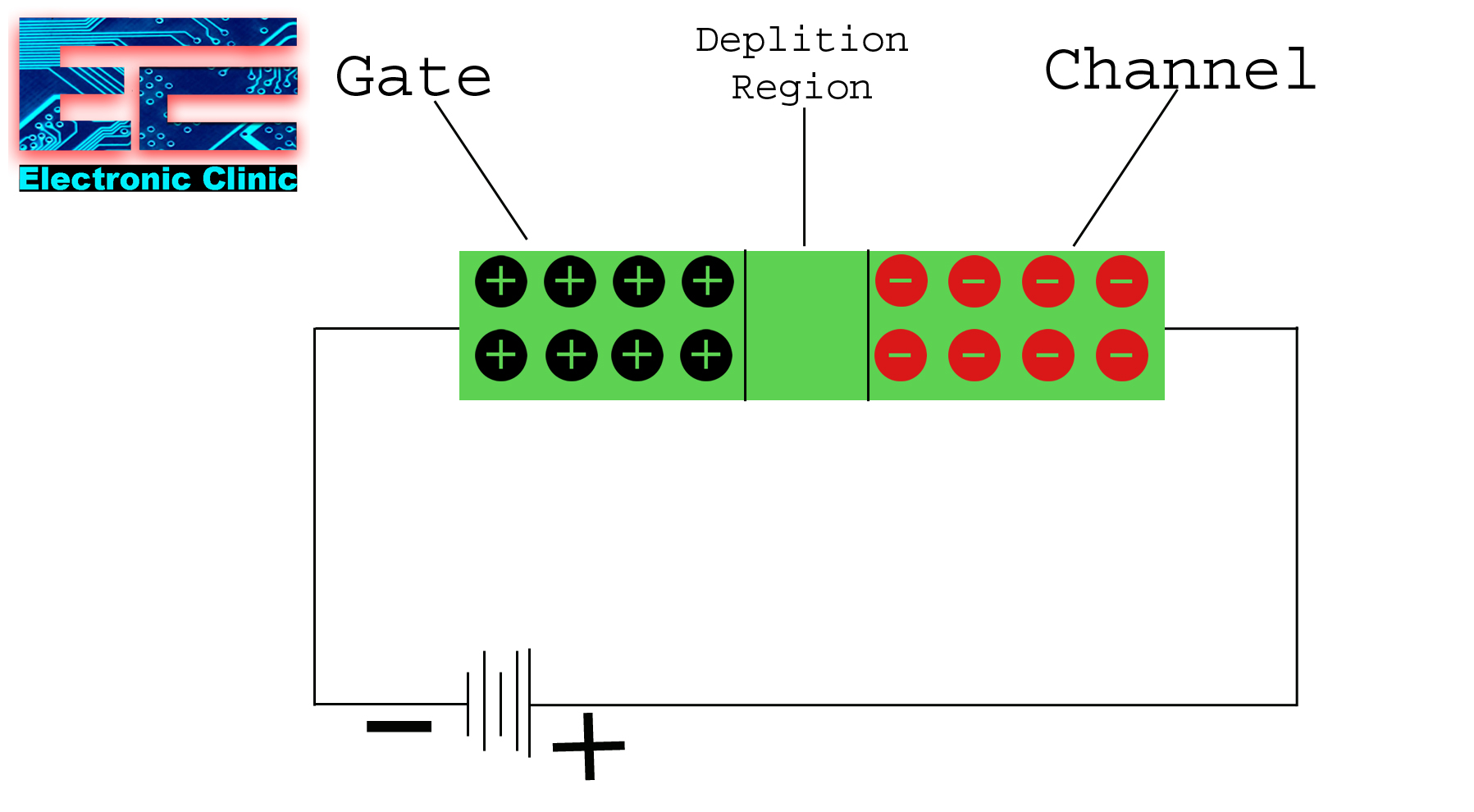
The voltage at which both the depletion regions touch each other called pinch off voltage and is denoted by Vp and is the point at which both depletion region touch each other is called pinch off point. At this voltage the current reaches to its maximum value and is called saturation current Denoted by Is. This current will remain same even if the voltage increases beyond Vp. Then break down occurs and Id increases abruptly to a very very large value.
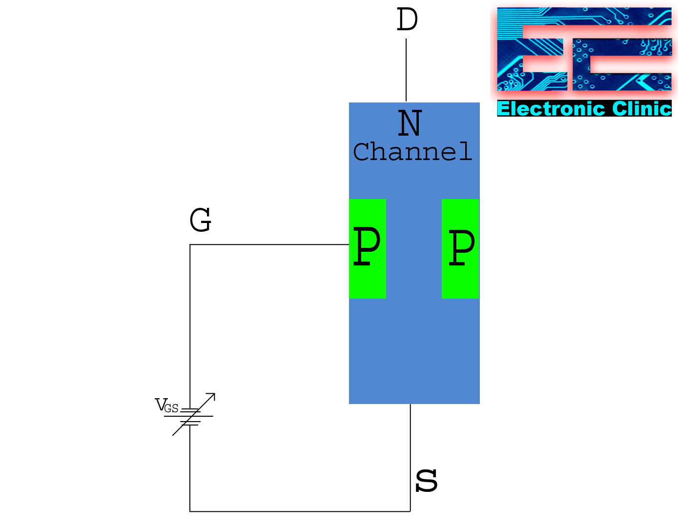
Now consider the drain terminal, apply +Ve voltage at drain terminal with Respect to source terminal, is VDS. The source terminal is connected with -ve terminal of voltage drain supply as shown in figure given below.
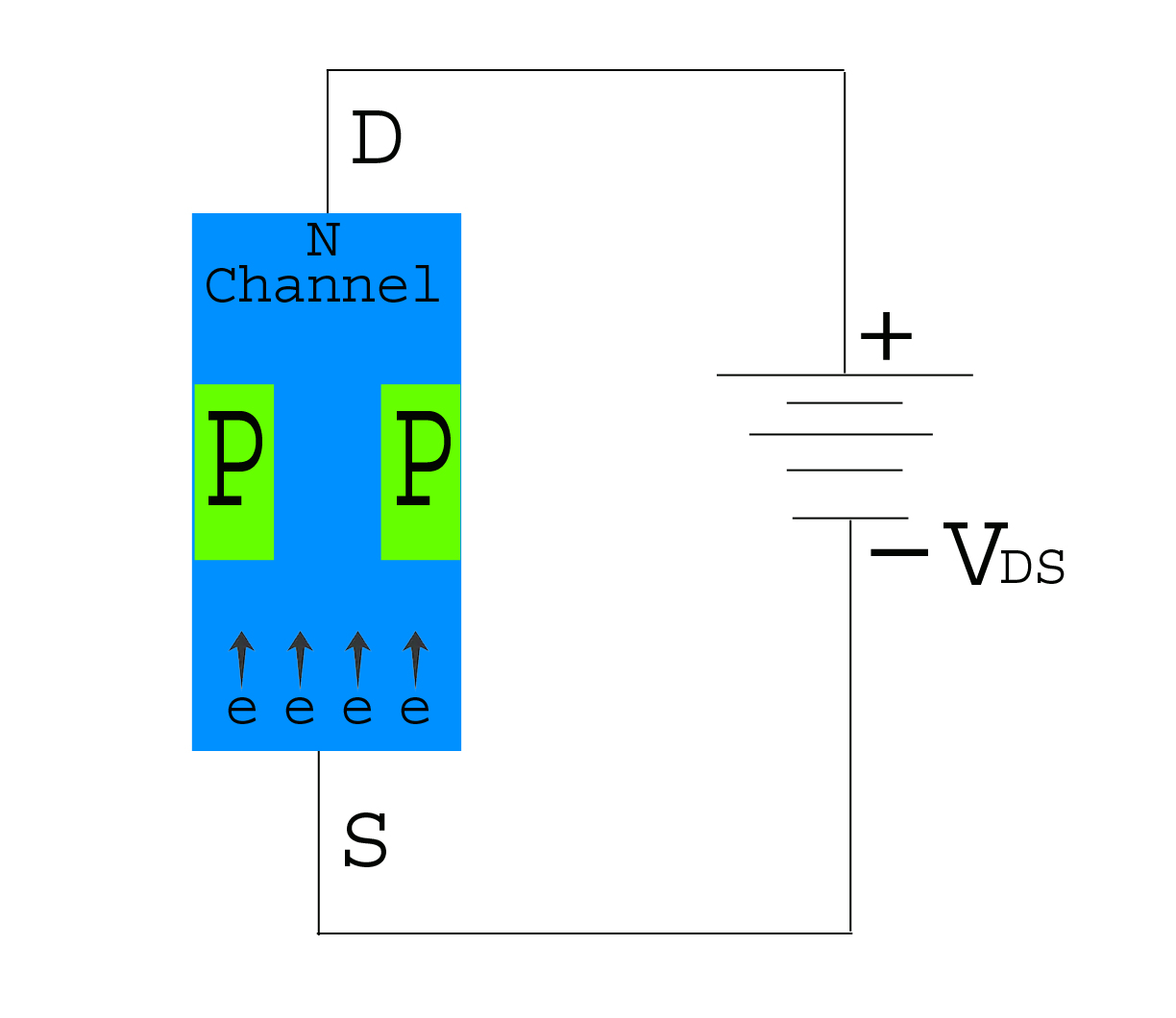
When potential difference is established b/w drain and source then free electrons will move from source to drain along the length of the bar through channel as shown in figure given below.
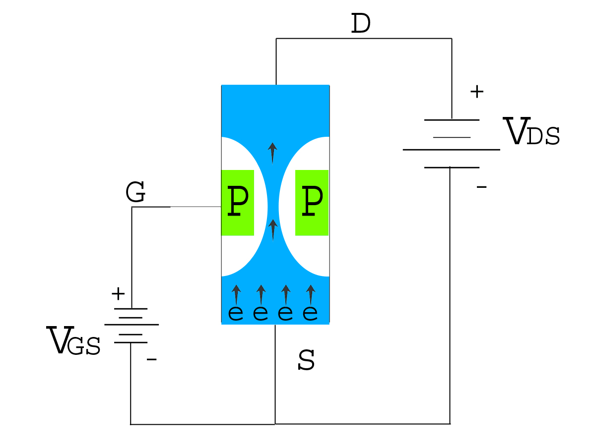
This flow of electrons will constitute drain current ID. This current “ID” is composed of majority charge carriers only and flow along the length of the bar through the channel (the conventional drain current will flow from drain to source through the channel)
For small drain voltage the bar behaves like a simple resistor. The resistance of the bar depends upon the doping, channel width, channel length, and channel thickness. For this the drain current increases linearly with the applied voltage that is ID increases with VDS (this increase is according to the ohms law, this linear increase will be up to some region. So the region where the linear Charge is maintained is called ohmic region).
Hence we can say that initially drain current ID depends on drain to source voltage. When VDS is gradually increased from zero then ID increases proportionally. By increasing -Ve voltage to the gate the depletion region increases and the width of the channel increases and the drain current “ID” also decreases.
It is observed that by increasing -Ve biased voltage at gate terminal the depletion region touches each other at the channel, it stops the flow drain current “ID”. So we can say that gate of JFET will control the drain current “ID”. The characteristic curve for the JFET is given as,
The curve b/w voltage and current is called characteristic curve.
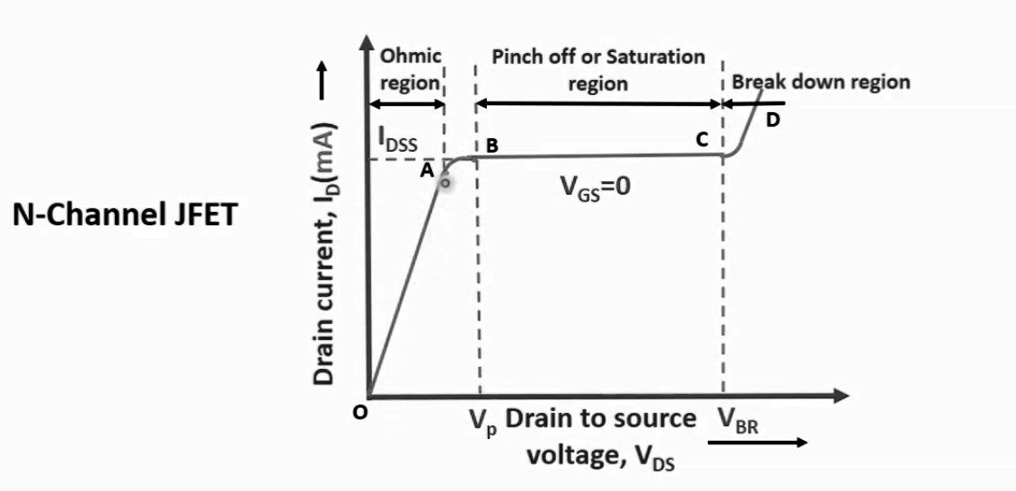
- Ohmic region (OA)
- Curve AB
- Pinch off region(BC)
- Break Down region(CD)
Ohmic Region:
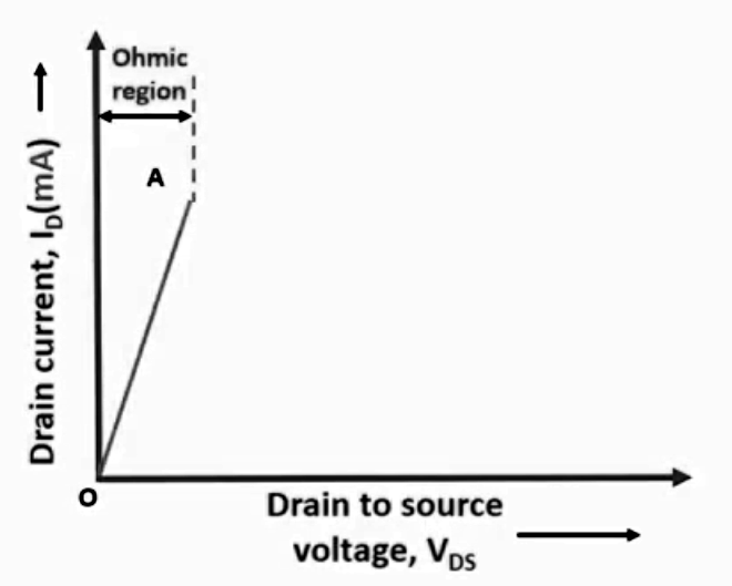
- The current ID increases linearly with VDS
- The device obeys ohms law
- As N-type Semiconductor bar acts s simple resistor
Cuve AB:
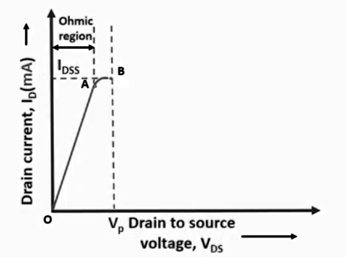
- With increase in VDS, the ID increase at inverse square law rate.
- The ID current increases slowly with VDS.
- B increases and D.L increases and channel width reduces
- At VDS corresponding to point B, the Channel reduced to minimum and is called as pinch off voltage(Vp)
- The drain to source voltage at which channel pinch off occurs is called as pinch off voltage(Vp).
Pinch off region(BC) (VGS=0):
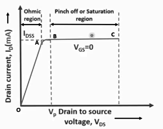
- This region is called constant current region or saturation region.
- The drain current remains constant at its max value IDSS.
- ID depends on VGS.
- The device used as an amplifier.
Break down region(CD)
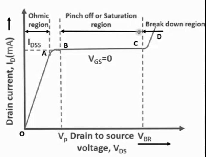
- The Drain current increases rapidly with drain to source voltage.
- As the Break down of G to S Junction occurs due to avalanche effect.
- The VDS corresponds to point C is break down voltage VBR.