PhotoTransistor Introduction, Construction, Working and Uses
Table of Contents
Photo Transistor Introduction:
A transistor the collector-base junction of which is very sensitive to light is called a phototransistor. When light casts on a collector-based PN junction (which is usually reverse bias) a base current produces in the junction by means of this light. The value of this current is directly proportional to the intensity of light falling on the junction. Remember that when light falls on transistors’ collector-base photo junction, its resistance reduces. In other words, a transistor from which the flow of current starts when light falls on its photo base junction is called a phototransistor. The input of such a transistor is in the shape of light instead of a base current. Actually, photo transistor is a device that is a collection of a semiconductor’s photo-responsive characteristics and an ordinary transistor’s amplifying capacities. That phototransistor is a PN junction device, which is commonly manufactured as a transistor. However, it is basically used as a photodiode. Remember that a phototransistor has two junctions compared to a photodiode. Base connections are formed with some of the phototransistors; however, no electrical connection exists along the base of most of the phototransistors.
Construction of Photo Transistor
From the construction viewpoint, phototransistors are constructed similar to an ordinary or conventional transistor with the help of silicone or germanium’s N or P semiconductors in a mutual NPN or PNP series. In figure 7.12, a silicon phototransistor, and in figure 7.13, the construction of a junction-type phototransistor has been illustrated. This unit consists of an NPN or PNP germanium wafer which has been set in such a way that light rays focus directly on the area of the base-emitter junction via a lens. As light rays are a substitute for input electrical signals, therefore there is no need for a base lead-in phototransistor. Remember that area of the collector-base junction of a phototransistor is larger compared to its emitter-base junction, so that maximum light rays could transmit on the junction (in other words, as the process of production of base current via light occurs in the collector-base junction of a phototransistor, therefore the area of this junction is set large comparatively, so that maximum base current could be generated). In figure 7.14 (a), a symbol of a phototransistor, and in figure (b), the construction of a definite transistor chip has been depicted.
Figure 7.12 (a) – the construction of a typical photo transistor 7.12 (b). NPN silicon phototransistor
Figure 7.13- construction of junction type photo transistor
Figure 7.14 (a). photo transistor symbol 7.14 (b). typical photo transistor chip structure
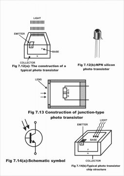
In figure 7.12, the construction procedure of an NPN transistor has been explained. First of all, an N-type substrate (which is usually silicone) is taken which acts as a transistor’s collector. A P-type segment is diffused in this N-type substrate, which works as a base. After this, an N-type segment is diffused in this P-type base which works as an emitter. Thus, an NPN phototransistor is formed which normally looks similar to a bipolar transistor. It is eventually closed in a transparent crust so that light may reflect on its upper surface. Similarly, a PNP photo transistor is designed in which an N-type segment is diffused in a P-type substrate. Finally, it is completed by diffusing another P-type segment in this N-type base.
A phototransistor may also have two leads. Or it may also contain three leads. No electric base is made in a two-type lead construction. Thus, two lead-type devices operate by just providing light as a means of input. However, a three-lead device has a base lead; so that it could be operated as a phototransistor during the availability of light. And at the same time, it may also be operated as an ordinary bipolar transistor in the absence of light. However, two lead transistors are most prominent in several applications.
In other words, a phototransistor also has emitter and collector wires apart from the base; however, base wire is used very rarely for any purpose. Through base, only the operating point of a phototransistor can be adjusted (that’s under various circumstances; collector-base current of a transistor is controlled via providing bias voltages to the base). However, mostly emitter and collector lead (wires) of phototransistors are used and it is assumed that this device has just two leads.
Operation or Working
An emitter-base junction of a phototransistor can be forward-biased just like an ordinary bi-polar transistor, whereas its collector-base junction is reversed bias. In figure 7.15, the bias circuit of a phototransistor and its peculiar characteristics curves have been shown.
Figure 7.15- phototransistor bias circuit and typical collector characteristic curves
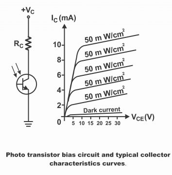
When light does not reflect on a phototransistor, a very minute quantity (in nano amperes) of the thermally generated collector to emitter current ICEO flows through it, which is known as a dark current. On the contrary, when the transistor’s collector-base junction receives light via a lens fitted on its junction, electron holes are generated as a result of light focusing on the collector’s base. Thus, the resistance of this region subsides and a base current generates is it proportional to the intensity of light. As a result of the generation of base current, collector current IC flows, the value of which enhances with increases in the base current. Remember that a phototransistor just operates like a conventional bipolar transistor with the exception of its ability to produce base current. Phototransistor generates current gain due to base current or photocurrent. Thus, the value of collector current received from a phototransistor is as follows:
IC = Iλ (β+1)
Here β means gain while Iλ means photocurrent or base current.
According to the afore-mentioned formula, output current or collector current received from a phototransistor equals the product of the intensity of light rays and the transistor’s gain. The gain of a phototransistor is normally ranged between 400 to 500. From the characteristic curves (which are drawn by plotting collector currents vertically whereas collector voltages horizontally) shown in the figure, it becomes evident that every curve reflects a peculiar intensity of light (in such a situation, the unit of light intensity is mil watts per square centimeter mW/Cm2) and collector current (IC) increases with increases in the intensity of light. Thus, the properties of a phototransistor are similar to an ordinary transistor with the exception that in a phototransistor, the intensity of light is taken into consideration instead of the base current.
When a phototransistor is fitted into a circuit, electron holes generate due to the reflection of light on the collector-base junction. As a positive potential is found on the collector, therefore electrons move towards the collector, which becomes a means for the flow of collector current, whereas holes remain on base, which causes a rise in the forward bias of the emitter-base junction. Thus, transistors’ current amplification gets high. The output current of a transistor can be enhanced by adequately increasing the area of the collector-base junction of a phototransistor, increasing the value of β, and increasing the light-absorbing capacity on the junction.
We have to remember that phototransistors are not sensitive to all forms of light. Rather, they only operate via light present inside a specific wavelength range.
The advantage of a phototransistor is that it delivers gain current. Therefore, it is about times as sensitive to light compared to a photodiode. That phototransistor provides inordinately high current output compared to a photodiode. However, its switching speed is less compared to the photodiode. Therefore, where ever a fast switching speed is desired, an ordinary high-speed switching transistor along with a photodiode is used instead of a phototransistor.
Uses
Due to excellent performance and extreme sensitivity, the phototransistor is used in relays on-off systems, computer cards, position locators, inter vision alarms, optical tachometers, level indicators, microcomputers, tape circuits, and optical coupled amplifiers. Moreover, it is also used in smoke or fire detecting appliances, counting gadgets, and mobile systems. Photo transistors’ response is comparatively less relative to photodiode; however, the advantage of amplification can also be availed from them. These are small-sized, strongly built, and have a long life.
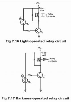
In figure 7.16, a relay circuit has been revealed that operates via light. Here photo transistor plays a basic role. When the light of an adequate wavelength falls on the base of phototransistor Q1, it starts conducting (i.e. phototransistor acts as an optical switch). Phototransistor Q1 drives bipolar transistor Q2. Thus, Q2 starts operating in its saturation region and its collector current passes via a relay coil (as shown in the figure). As a result, the relay gets energized or it turns on (that’s its normally open contacts close and normally closed contacts get opened). Thus, a relay can be operated via the reflection of light on the phototransistor fitted on the circuit.
In Figures 7.17, and 7.17, a circuit has been displayed wherein sheds light on a phototransistor; a relay can be de-energized or turned off. When light falling on a phototransistor is insufficient, transistor Q2 turns on, by means of which, the relay gets energized. When an adequate quantity of light falls on photo transistor Q1, it turns on. As Q1 turns on, the base of Q2 becomes low. Thus, Q2 turns off. As Q2 output is delivered on the relay coil, therefore, a relay also de-energizes as soon as Q2 turns off. These relay circuits can be used in different places for several objectives e.g. automatic door activators, process counter,s and various alarm systems, etc.
Figure 7.16
Figure 7.17
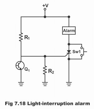
Another application of phototransistor has been depicted in figure 7.18. The phototransistor fitted on the circuit normally remains on (i.e. reasonable light falls on it all the time), as a result, SCR gate remains low (i.e. as long as phototransistor is on, no pulse is produced on the SCR gate and SCR remains off). Whenever light reflecting on the photo transistor disrupts due to any reason, phototransistor turns off. Thus, due to high transition on phototransistor collectors, SCR triggers. The alarm mechanism of SCR gets off the moment it triggers. This alarm can be RESET by momentarily pressing switch SW1 which has been fitted parallel to SCR. With the help of this circuit smoke and intrusion detection of any other type becomes possible.
Figure 7.18- light-interruption alarm
Previous Topic: Light Activated SCR or LASCR construction and working
Next Topic: Optocoupler Construction
For electronics and programming-related projects visit my YouTube channel.