How Prototype PCB Assembly Accelerates Product Development
Last Updated on March 6, 2025 by Engr. Shahzada Fahad
Table of Contents
Introduction:
How Prototype PCB Assembly Accelerates Product Development- Today’s electronic devices have become faster and more multi-functional, allowing synchronization, storage and accessibility in many industries such as automotive, aerospace, commercial and industrial. Take the example of efficient manufacturing systems where remote and automated monitoring of machines is now possible with the help of sophisticatedly connected devices.
If you rip apart these computers and smart consoles, you will find Printed Circuit Boards or PCBs that contain multitudes of electronic components with thin conductive traces that are intricately designed. These devices are not as simple as they seem on the exterior. Products such as electronic boards go through rigorous planning, designing, fabrication and assembly before they are placed in small enclosures. The product development stage is very essential in producing parts that will meet the requirements and shall last according to their intended lifecycle.
In this blog article, we will deeply explore and appreciate the world of prototype PCB assembly and how it helps accelerate product development.
What is Prototype PCB Assembly?
Prototype PCB assembly refers to the evaluation of the PCB design through the actual assembly of the printed circuit boards on a small volume. It is a crucial step to assess and test if the design has met the expected output response. In this early stage, the robustness and manufacturability of the PCB is also determined.
Printed Circuit Boards have a wide range of complexity from a single layer to multiple layers of conductive and insulative parts, thus, the cost of prototyping can also vary greatly depending on the design requirements, processing steps and testing. Prototype circuit board assembly is beneficial in accelerating product development as weaknesses in the design can be spotted ahead of mass production.
What is the Step-by-Step Procedure in Prototype PCB Assembly?
Every Prototype PCB assembly project follows a series of processes to come up with a working PCB prototype:
Design and Layout
Prior to the actual design and layout of the printed circuit boards, objectives must be clearly specified. An Electronic Design Automation or EDA software is used as a simulation tool to build schematics showing how components are interconnected. Next, is the physical arrangement of the components as to how they will be assembled on the actual board. The routings and stack-up consisting of the signal, power and ground layers are also planned on.
Design Simulation and Testing
Using simulation software, the layout and schematics are verified if they work as intended. Then a Design Rule Check is run to determine if the design is compliant with rules and guidelines. This step helps assess if the design is within the manufacturability of the PCB.
Prototype PCB Fabrication
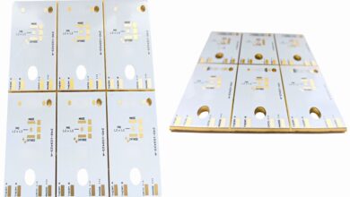
Manufacturing files, in a Gerber file format, are sent to the PCB fabrication supplier to commence with the PCB production. The bare PCB is first fabricated through a series of lamination, etching, drilling, plating and surface finishing processes. The bare PCB is electrically tested to check for any issues. For prototyping PCB, only small batch quantities are fabricated.
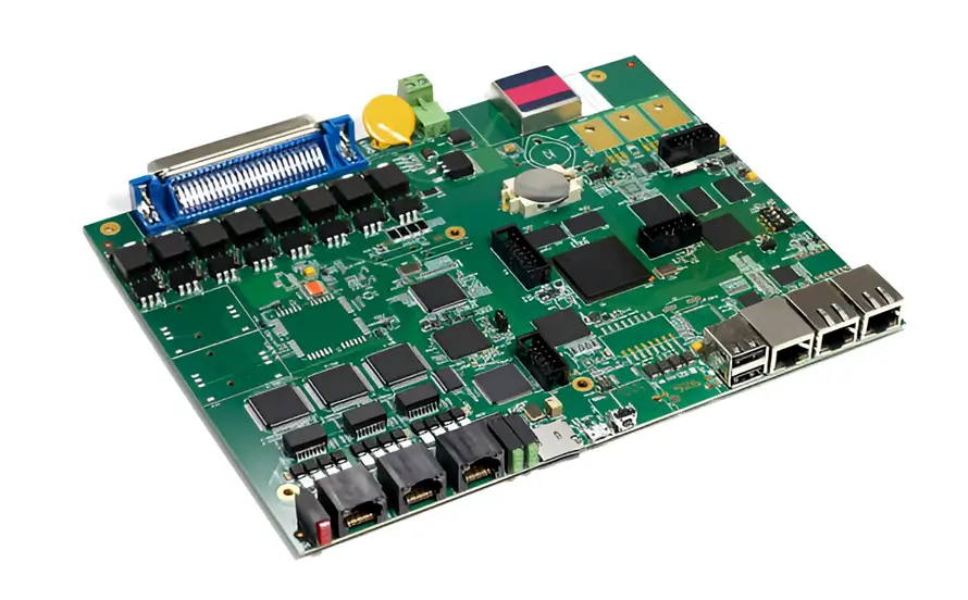
Prototype PCB Assembly
The prototype PCB assembly involves mounting the electronic parts, both passive and active components onto the bared PCBs. Prototype printed circuit board assembly has the following series of processes:
- Screen Printing. Solder paste is screen printed into the PCB to join the components with the contact pads. The volume and alignment of the printed paste dictate the soldering quality during this step.
- Component Placement. Electronic parts are placed into the PCB contact pads with the screen-printed paste. The accuracy of the placement is vital to avoid bridging or shorting issues between adjacent components.
- Reflow. The solder paste is heated and cured to form a reliable metallurgical bond. An oven with Nitrogen gas is pre-loaded with the thermal profile program with defined temperature and time settings.
Testing of Assembled Prototype PCB
The functionality of the printed circuit boards should be verified using electrical testing methods. Small batches of prototype PCBs normally use Flying Probe Testing as it utilizes a moveable probe that can access through components.
How Does Prototype PCB Assembly Accelerate Product Development?
Prototype PCB assembly can significantly impact the overall project in terms of cost, resources and timeline. China PCB assembly has already stood out in this field。 Below are the ways by which prototype circuit board assembly can help accelerate product development.
- Design Errors are Detected Immediately. Prototype printed circuit board assembly will help reveal design errors— whether the product is not working at all or there should be omissions in the design. In this systematic way, product development will not encounter further delays in the later phases of production. Improvement can be implemented immediately.
- Testing of Components and Overall PCB Performance. Part of the prototype circuit board assembly is testing the final assembled product before incorporating it into the final enclosure. Software simulation tools are available but not all-encompassing. Producing prototype PCBs and testing are detrimental to knowing if the individual component and overall PCB can perform well according to objectives.
- Early Time-To-Market. Issues that may arise because of skipping the prototyping phase can interfere with a faster introduction to the market. With prototype circuit board assembly, fixes are made early resulting in expedited decision-making. Prototype printed circuit board assembly also gives you more idea about the product which can be applied for future variants as a benchmarking strategy.
- Cost Management. An acceptable design should not just perform accordingly, it should also be within your cost objectives. With prototype printed circuit board assembly, cost trade-offs are further understood. In building a prototype, many significant decisions can further be made, such as higher cost in exchange for a product feature, or a lower cost by eliminating or replacing some parts of the design.
- Optimized Design. Do not expect that once you have the PCB design, everything will go smoothly once it runs in mass production. Often, design iterations are needed to correct, improve and enhance the design. Some design optimizations include changing materials, updating the routing layout and revising the dimensions. These design updates are necessary to improve the performance of the PCB or reduce the cost.
Discover more from Electronic Clinic
Subscribe to get the latest posts sent to your email.