Types of Multi-vibrator: Astable, Monostable and Bistable Vibrator
Last Updated on August 5, 2025 by Engr. Shahzada Fahad
Table of Contents
Types of Multi-vibrator
There are following three types of a Multi-vibrator.
(1). An Astable Multi-vibrator
(2). Monostable Multi-vibrator
(3). Bistable Multi-vibrator
Astable Multi-vibrator
In an astable multi-vibrator (AMV) device, neither of the two states/modes is stable or a Multi-vibrator device, none of the outputs of which is stable (i.e. both its states or modes are unstable). Rather it comprises two semi-stable (half-stable) states. Astable Multi-vibrator circuit continuously provides oscillation between these two states without any sort of excitation (i.e. it offers a continuous specific time-bound output pulse without the application of a trigger pulse). In simple words, an astable Multi-vibrator moves back and forth continuously between its two half-stable states. As a result of continuous movement between both its external states, an astable Multi-vibrator produces an unceasing time-specific signal (which continuously keep changing between 0 and 1 on its output. This signal is normally a squared type, as has been illustrated in the figure 6.4. Owing to creating a square-typed waveform, it is also known as a square wave generator and due to an incessant movement between its two output states, an astable Multi-vibrator is also known as a free-running Multi-vibrator (i.e. an astable Multi-vibrator circuit can be used as an oscillator or a generator). This circuit is simple, cheap and in case there is no issue of frequency stability, it happens to be a very apposite sort of generator. Remember that this circuit consists of two storing elements (i.e. two capacitors).
Figure 6.4-AMV

Monostable Multi-vibrator
Monostable Multi-vibrator (MMV) is also known as single-shot or single-swing or one-shot Multi-vibrator. A monostable Multi-vibrator, as the name suggests, consists of a stable state and a semi-stable state. And when an external trigger pulse is exerted on it, it switches from one-state to semi-stable state and after remaining on this state for some time, reverts back to its original state.
In other words, a monostable Multi-vibrator can remain stable on just one state and on any other state it becomes semi-stable or unstable. When it is being energized (suppose it is on its stable state) it remains on its stable state until some external trigger pulse is applied on it. On providing an extrinsic trigger pulse, monostable Multi-vibrator switches to unstable state. When trigger pulse ceases, it returns back automatically to its stable state (after the passage of some specific time). Trigger pulse changes the state of a monostable Multi-vibrator only temporarily. The period of time or duration during which it remains on an unstable state, is determined via values of components used on the internal circuit of a monostable Multi-vibrator. Remember that this circuit comprises a storing element (i.e. a capacitor) and this circuit is used as a pulse shaper, because it receives pulses of varying breadth on input and converts them into output pulses of same breadth. As its output state changes at a fixed time after provision of a trigger signal, therefore it can also be used as a delay element. Operation of a monostable vibrator has been illustrated vide figure 6.5.
Figure 6.5-MMV

Bistable Multi-vibrator
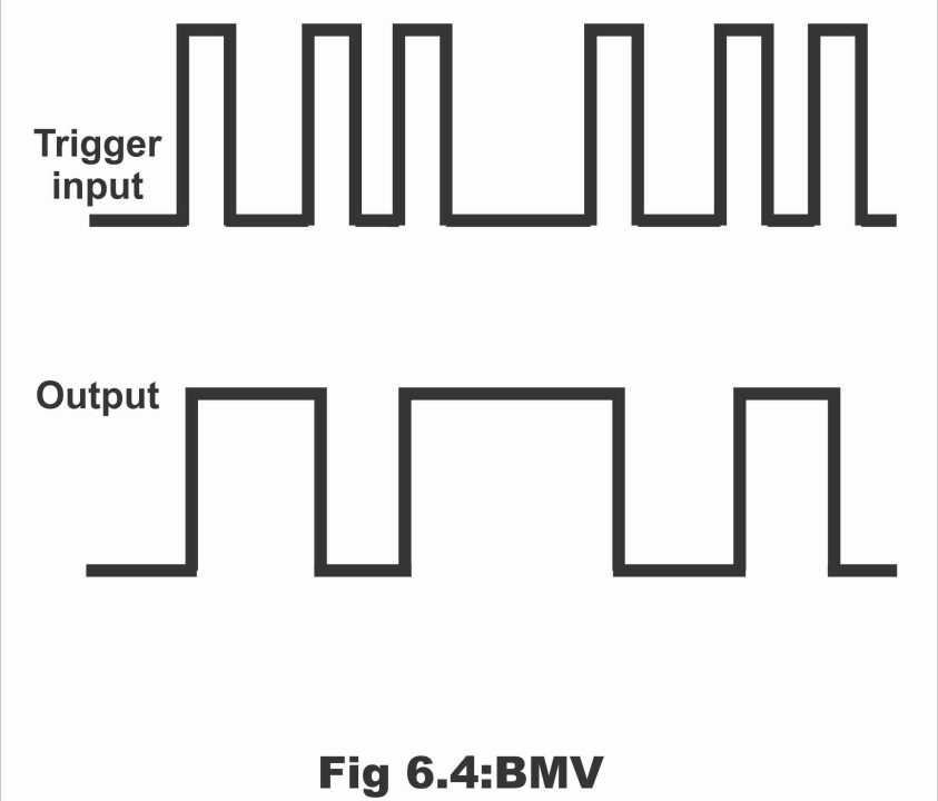
A Multi-vibrator which consists on two stable states or two stable outputs, is called bistable Multi-vibrator (bi means two). This Multi-vibrator remains on either of the two states until some extrinsic trigger pulse interferes and changes it to other state (i.e. trigger pulse can cause a change in Multi-vibrator’s state or output and as long as trigger pulse is not received, it retains one of its state). In other words, it may also be said that this bistable Multi-vibrator recognizes its previous output. As a flip-flop has this particular quality therefore, a bistable multi–vibrator is also known as a just flip-flop or flip-flop Multi-vibrator. Moreover, it is also known as binary or divided-by-two elements. Remember that no storage element exists in a bistable Multi-vibrator (BMV) nor does it oscillate.
In figure 6.6, operation of a bistable Multi-vibrator has been illustrated.
555 Timer
555 Timer is a digital monolithic integrated circuit that can be used as a clock generator. In other words, it is a digital timing circuit, which can be connected as an astable or monostable circuit. A 555 timer is a versatile type and a massively used device, which operates on any one of these two states i.e. either an astable or monostable state. It can provide a time delay ranging from few micro seconds to several hours. As this device (i.e. 555 timer) can be used both as an astable as well as monostable circuit, therefore it is called a timer. A 555 device is a low-priced device, which is available in the form of an IC. It operates within a pretty vast range of potential difference (normally between +4.5V to +15V) and there is no effect on output either of these changing voltages. That’s why it is also called a linear device. Due to being compatible, a 555 timer can directly be connected with TTL or CMOS digital circuits. However, in order to connect with other digital circuits, interfacing is always required.
Various organizations produce different type of 555 timers, amongst which, the basic number is 555. For example, SE555, CA555, SN555 and MC14 555 etc. Two 555 timers are generally fabricated within one chip and it is allotted 556 number. Now-a -days such types of 555 are also commonly available, on one chip of which four 555 timers exist. These devices are available in the form of 8-pin round IC, or in the shape of a DIP containing 8 pins or 14-pin shaped DIP.
In figure 6.7, pin diagram of 555 timer consisting on an 8-pin DIP (dual inline package) has been demonstrated. The pins detail of this IC is as under:
Figure 6.7-pin diagram of 555 timer having 8-pins

555 Time Pin Description:
(1). Ground
It is common ground point of a circuit. Along with ground terminal of an extrinsic circuit, ground terminal of the power supply (VCC) is connected with this common ground point.
(2). Trigger
When a negative trigger pulse equivalent to 1/3 of a total VCC voltage (i.e. VCC/3) amplitude, is provided on this terminal, output state of the circuit switches from low to high.
(3). Output
Output is acquired through this terminal and this terminal is connected with load. The terminal can either be low or high at a time.
(4). Reset
Irrespective of previous output state, providing a trigger pulse on the terminal, resets the device (i.e. output turns out to be low)
(5). Control Voltage
Two third (2/3) positive VCC voltage of an overall VCC voltage, exist on this terminal. Thus, it becomes a part of a comparator circuit. Normally, a capacitor is mounted between this terminal and ground.
(6). Threshold Voltage
Threshold voltage and control voltage are two input voltages of a comparator circuit. Circuit compares voltage levels present on the circuit terminal with reference to voltage present on the control terminal. If threshold voltage existing on pin number 6 exceeds control voltage (equivalent to 2/3 of VCC), output turns low. And if voltage of pin number 6 is less as compared to control voltage, output turns high.
(7).Discharge
When output is low, this terminal provides a low resistance discharge path to the extrinsically fitted capacitor. However, when output is high, this terminal operates similar to an open circuit.
(8). Supply Voltage Terminal +VCC
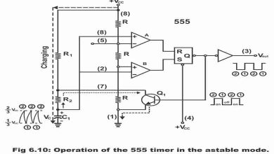
Supply voltage are applied on the terminal in order to drive or operate a 555 timer. In figure 6.8, a simple diagram of 555 timer has been illustrated, by means of which its intrinsic circuit has been explained. According to this figure, this timer consists of two comparators, an RS flip-flop, output stage (output buffer) and a discharge transistor Q1. It also contains three resistors mounted on 5KΩ series, one end of which is connected with +VCC (i.e. with pin number 8) and other point or end connected with ground (GND) or pin number 1. Remember that owing to three resistors being fitted on a 5KΩ series, this IC timer chip has been named as 555.

Working Method
Comparators present in the functional or block diagram of a 555 timer are devices, output of which is high when its positive input voltage is high as compared to negative input voltage. And comparator output is low when negative input voltage comparatively exceeds positive input voltage. The voltage divider in the circuit consists of three resistors of 5KΩ, which provide 1/3 trigger level of VCC (i.e. 1/3 VCC) and 2/3 threshold level of VCC. In order to understand this point, let us suppose that value of VCC is 15. In such a situation, trigger level value is 5V (1/3 x15 = 5) and threshold level value 10V (i.e. 2/3 x 15 = 10V). If there is a need to extrinsically adjust trigger level and threshold level on some other voltage level, then control voltage input (pin number 5) is used for this purpose (i.e. trigger level and threshold level voltages can be changed when required by means of changing input control voltage of pin number 5). However, it must be remembered that in such a situation, value of trigger level be equal to 1/3VCC and value of threshold level equal to 2/3VCC. The process of circuit operation is as follows:
When value of normal high trigger input falls below 1/3VCC momentarily, then comparator B ‘s output rises from low to high. As a result, RS latch or RS flip-flop becomes set. As a result of a set flip-flop, output (pin number 3) gets high and simultaneously, discharge transistor Q1 turns off. This output tends to remain high so long as the normal threshold input value does not exceed to 2/3 VCC. As soon as, threshold input value exceeds 2/3 VCC, comparator A output turns from low to high. As a result of a high comparator value, RS flip-flop resets (as comparator A ‘s output is directly associated with R input of the RS flip-flop, as has been shown in the figure). As soon as flip-flop resets, output turns low once again and discharge transistor Q1 turns on. Flip-flop can also be rest without a threshold circuit via application of an extrinsic reset input. Remember that trigger and threshold inputs (pin 2 and pin 6) are controlled through extrinsic components. And by means of this control through these threshold and trigger inputs components, this timer can be used for an astable or monostable action.
Previous Topic: Types of Clock: Discrete Components and Integrated Circuit TTL Clock
Next Topic: 555 Timer as an Astable and Monostable Multi-Vibrator with circuit diagram
For electronics and programming-related projects visit my YouTube channel.
Discover more from Electronic Clinic
Subscribe to get the latest posts sent to your email.