Types of Clock: Discrete Components and Integrated Circuit TTL Clock
Last Updated on November 21, 2022 by Engr. Shahzada Fahad
Table of Contents
Clock
A clock is a circuit, which provides such periodic or definite signals on a logic circuit or digital system, which tends to change its operational mode or condition. Remember that these signals are used in order to synchronize different digital circuits or computer operations. In other words, circuit provides such a continuous periodic (containing specific intervals) waveform (normally square or quadratic shaped waveform) which is used to synchronize signals in a digital system, is called clock or timer.
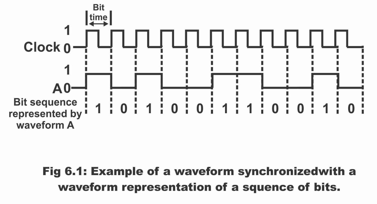
In fact, clock may be treated as a heart of any digital system, as it provides heartbeat for the system and without which, system virtually gets blocked or stops working (i.e. significance which heart has in a human body, same is the importance of a clock in any digital system). All waveforms within multiple digital systems are synchronized via a rudimentary timing waveform, which is called clock. Clock is a periodic waveform wherein space or gap between pulses (which is called interval or period) is equal to a time bit. This has been demonstrated via clock waveform or clock signal as shown in figure 6.1. It has to be inculcated that every time, a change takes place on A waveform level on the leading edge of clock waveform (i.e. a waveform has been synchronized with a leading edge of the clock waveform or clock signal or clock pulse). However, in certain instances change can also occur in levels on the trailing edge of the clock. During every clock time bit, waveform is either high or low. As such clock or timer is such a circuit, which provide square or rectangular type periodic waveforms (or provides such a signal), which are used as a basic timing signal in digital circuits.
Remember that pulses which are received from clock and applied on a logic circuit, are called clock pulses and the pulse operation is referred to as clocking. Moreover, circuits which operate or work on the basis of these signals or pulses, are called clocked circuits or synchronous circuits. Further, frequency received by means of a clock, is called clock frequency. The circuit from which square or rectangular-shaped signals are produced, is called clock oscillator and a specific frequency produced via the oscillator’s pulses is termed as duty cycle or amplitude. Clock output is normally provided on sequential logic circuits. As soon as clock output is transmitted on these circuits, their normal working condition change. Thus, these logic circuits perform the desired operation in accordance with design of clock’ s output. Practically, some sort of an astable multi–vibrator is used in all circuits of a digital clock oscillator in order to produce periodic waveforms. There are two unstable conditions of these type of circuits and these circuits recurrently keep switching between these two states.
Figure 6.1 – example of a clock waveform synchronized with a waveform representation of a sequence of bits
Types of Clocks
(1). Discrete Components Clock
(2). Integrated Circuit TTL Clock
Discrete Components Clock
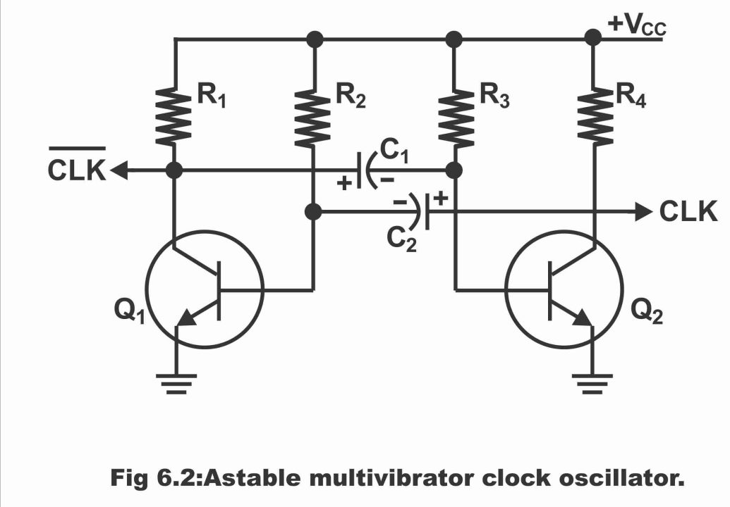
Clocks which are manufactured by means of interconnecting discrete components, are called discrete component clocks. In figure 6.2, a commonly used a-stable multi-vibrator clock oscillator circuit has been depicted, which contains two transistors Q1 and Q2, two capacitors C1 and C2 and four resistors R1, R2, R3 and R4. Both the transistors present in this circuit, are used as invertor and output of one transistor has been linked with input of the other transistor. Resistors R2 and R3 fixed along the base of both transistors, provide bias on the corresponding transistor in a saturation state. Whereas capacitors C1 and C2 connect one inverter’s output with input of another. Remember that as an astable multi-vibrator has two unstable conditions, therefore when a transistor conducts under normal circumstances (i.e. turns on) other transistor does not conduct at that time (i.e. it remains off) and output of this clock oscillator keeps changing between supply voltage +VCC and +V(SAT) of both transistors.
Figure 6.2 – An astable multivibrator clock oscillator
Operation
First of all, presume that transistor Q2 has been conducting, whereas transistor Q1 is off. In such a situation, capacitor C1 (which is connected with base of Q2) keeps charging up to +VCC via Q2 emitter–base (E/B) junction and R1. It has to be kept in mind that prior to this, capacitor C2, which has been charged till supply voltage, cuts – off C1 under such a situation and this capacitor keeps discharging through R2 at that moment. As soon as capacitor C2 has been completely discharged, it starts charging again immediately in its reverse direction. When charge value on C2 equals to near 0.7V, transistor Q1 begins to conduct (because 0.7V are required to charge a silicon transistor). As soon as Q1 begins to conduct, positive plate of capacitor C1 (which is connected with collector Q1), becomes grounded, by means of which negative voltages intrude between Q2’s base and emitter. As a consequence, it turns off immediately. At that time, C1 capacitor connected along Q2 base, starts discharging via resistor R3. At that moment, capacitor C2, starts to re – charge via transistor Q1 emitter – base junction and resistor R4. Thus, as soon as C1 charge turns out to be 0, it kicks – off recharging up to +VCC. As soon as C1 voltages turn high to a reasonable limit (i.e. 0.7V), Q2 begins to re–conduct (because these charged voltages of capacitor C1 are transmitted on Q2’s base), as a result, circuit’s condition changes. This conduction operation of Q1 and Q2 by turns, goes on continuously. its rate depends on the discharge time of C1 and C2 capacitors and values of R2 and R3 resistors. Remember that oscillation frequency (f) of this clock oscillator is determined via values of C1, C2, R2 and R3. Further, R2 and R3 values are selected in such a manner that Q1 and Q2 saturate. This clock oscillator circuit can directly drive standard type logic circuits (TTL and CMOS). However, in order to operate other type of logic circuits by means of this clock oscillator, an interface is being applied between this clock oscillator and the corresponding logic circuit (the device mounted between two digital circuits or systems for synchronization purposes is called interface).
Transistor-Transistor Logic Clock
TTL clock is a circuit which produces clock waveforms which are compatible with a standard TTL logic circuit (or are suitable for standard TTL circuits)
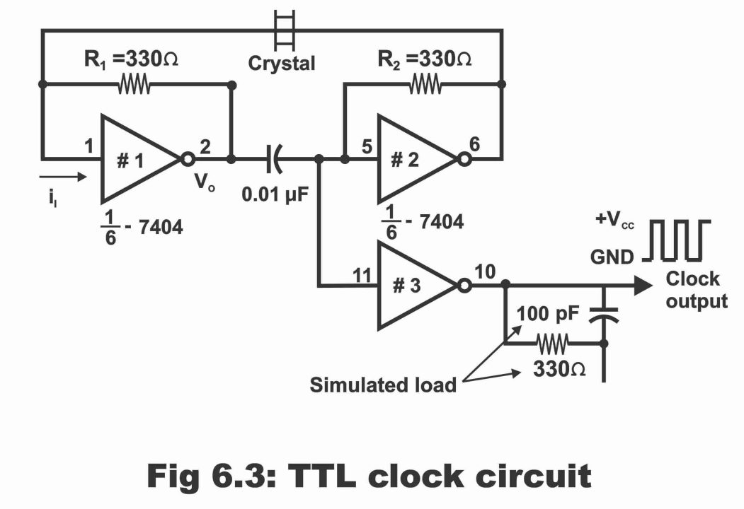
Applying a 7404-hexadecimal inverter, a quality TTL compatible clock can be manufactured, as has been illustrated in figure 6.3. This clock circuit is quite common and massively being used. A two–stage amplifier is constructed by means of applying two inverters on this circuit, between pin 1 and 6 of which, an overall phase shift of 360° exists. Some portion of signal found on pin 6 is feedback/ passed back on pin 1 by means of a crystal. Thus, this circuit produces oscillations in accordance with crystal frequency. As feedback element is crystal, therefore oscillation frequency tends to be fairly stable.
Fig 6.3 – TTL clock circuit
Operation or Working
A feedback resistor of 330Ω has been connected with output of inverter 1 (pin number 2) and input (pin number 1), by means of which a current–to–voltage amplifier is constructed. Its gain is as follows:
A1 = V0/Ii = -R1
Remember that a minus sign along R1, represents 180° phase shift. As R1 value is 330Ω, therefore its amplifier gain is as under:
A1 = -330 V/A
For example, if an addition of 1mA is done in input current Ii, then value of negative going voltage on V0 will be as under:
A1 = V0/Ii or V0 = A1 Ii = 330 x 1mA = 330mV
As inverter 2 has also been mounted similar to inverter 1, therefore its gain is equivalent to -R2 (i.e. A2 = -R2). In the circuit, both amplifiers have been AC coupled with 0.01µF capacitor (because this capacitor lets AC current pass through it). As a result, both amplifiers develop an amplifier gain, overall gain of which is as follows:
A = A1 x A2 = (-R1) (-R2) = R1 R2
It must be remembered here that overall gain happens to be positive, which indicates an overall shift gain of 360° (because phase shift of first amplifier is -180, similarly phase shift of another amplifier is also -180. As both amplifiers have been coupled together in order to form a two – stage amplifier, therefore phase shift of this amplifier equals to total phase shifts of both the amplifiers i.e. 360°). Thus, in such a situation, overall gain is as follows:
A = 330 x 330 = 1.09 x 10⁵ V/A
Now if 45µA is added to input current Ii, in such a situation +5V are received on pin number 6 of inverter 2. Now if some portion of signal from pin number 6 is feedback on pin number 1, in such a condition, ii will increase (due to a positive feedback) and circuit will begin to oscillate (i.e. circuit starts producing oscillation)
In order to feedback some portion of signal from pin 6 to pin number 1, a series mode crystal is being used. This crystal functions analogous to a series RLC circuit and it behaves like an ideal low resistance element on resonance, wherein no phase shift exists (remember that in situation of resonance, overall reactance of such a circuit is zero owing to inductive reactance and capacitive reactance being mutually equal. The impedance of an RLC resonant circuit equals to its resistance and its current tends to be in – phased with respect to the applied voltage. Further, power factor of this circuit is unity and maximum current value passes through it). Thus, feedback signal must be resonance enduring (so that phase – shift could be avoided). And both inverters along with crystal should build such an oscillator which operate on crystal resonant frequency (because, oscillation frequency is set by means of crystal)
Overall gain owing to the feedback element mounted along the circuit turns out to be such, that it can drive every inverter between saturation and cut – off region. Thus, output signal is transmitted in periodic waveform shape, as has been illustrated in the figure. The clock signal transmitted on output keeps changing between 0 and +5V in less than a 10 nano seconds time. As a result of sudden wave fluctuations (rise and fall), a square wave is obtained. The frequency of this clock signal can be determined through a crystal and its waveforms normally range between 1 MHZ and 20 MHZ.
Invertor number 3 as shown in the figure, has been used as a buffer amplifier or an isolation amplifier on output (buffer means a circuit which blocks input and output loading) and it drive a load of 330Ω fitted parallel to 100PF, whereas rise and fall time remains less than 10 nano seconds as usual.
Timers
Timers are circuits which provide periodic signals on some digital system, by means of which a system’s status changes. In other words, circuits which operate on the basis of changes taking place in a multi-vibrator mounted on a circuit, are called timers. In other words, a device which can be used as a multi-vibrator circuit, is called timer. Whereas multi-vibrator is such a circuit which can provide just two possible outputs i.e. high level and low level and besides these two levels, no third level exists. In other words, an electronic circuit, which consists of two output terminals, and the voltage level of one output terminal is always different from the voltage level of other output terminal, is called multi-vibrator. For example, if two voltage levels are 0V and 5V, then one of the multi – vibrator’s output is on 1 whereas its second output is on 5V at a time.
Multi-vibrators are fundamentally two-stage amplifiers wherein output of one of the amplifiers is connected to the input of other amplifier in order to provide a positive feedback. This feedback is provided in such a manner that at a time, only one of the transistors can saturate or turn on, whereas other transistor remains cut–off. After this, a new state forms or builds up on multi-vibrator, according to which the transistor which was saturated in the first instance, now turns to be cut-off. While the transistor which was initially in cut–off mode, now switches to saturation mode. Remember that these devices are commonly used as pulse generating, storing, and counting circuits.
Previous Topic: Trigger in Flip-Flop with Circuit Diagram in Digital Electronics
Next Topic: Types of Multi-vibrator: Astable, Monostable and Bistable Vibrator
For electronics and programming-related projects visit my YouTube channel.
Discover more from Electronic Clinic
Subscribe to get the latest posts sent to your email.