8085 Microprocessor Architecture in Digital Electronics
Last Updated on April 18, 2023 by Engr. Shahzada Fahad
8085 Microprocessor
The 8085 microprocessor manufactured by Intel Corporation is a better and developed version of its own manufactured 8080 microprocessor. Instruction sets for both 8080 and 8085 types of microprocessors are the same, except addition of two instructions that have been inducted into 8085. Apart from additional instructions, 8085 microprocessor has multiple extra registers as compared to 8080 microprocessor. The essential components being used in a 8085 microprocessor are as follows;
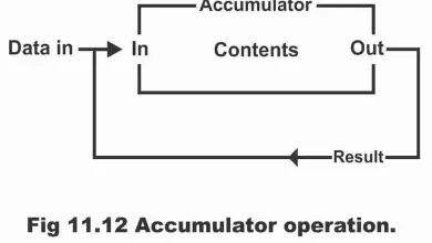
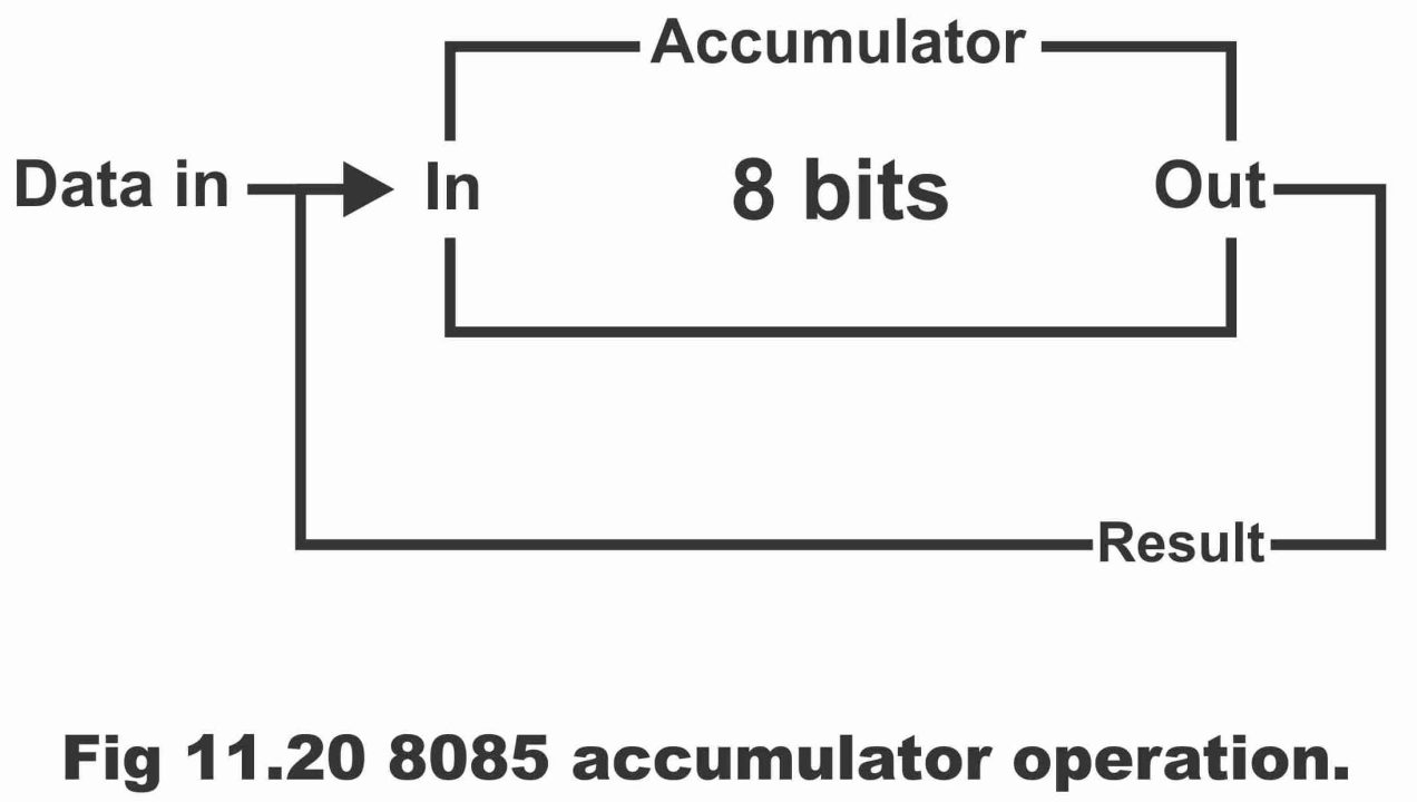
Accumulator
We know that an accumulator is a storage place or register (its details have been provided above). The chip of an 8085 microprocessor consists of an 8 – bit accumulator. Its operation has been illustrated in figure 11.20.
Figure 11.20 – 8085 Accumulator model
General Purpose Registers
The general-purpose registers exist on a 8085 microprocessor chip, in abundance and these registers are organized in the shape of pairs. The configuration of one pair out of multiple pairs has been illustrated vide diagram 11.21.
Figure 11.21 – Model 8085 general–purpose register
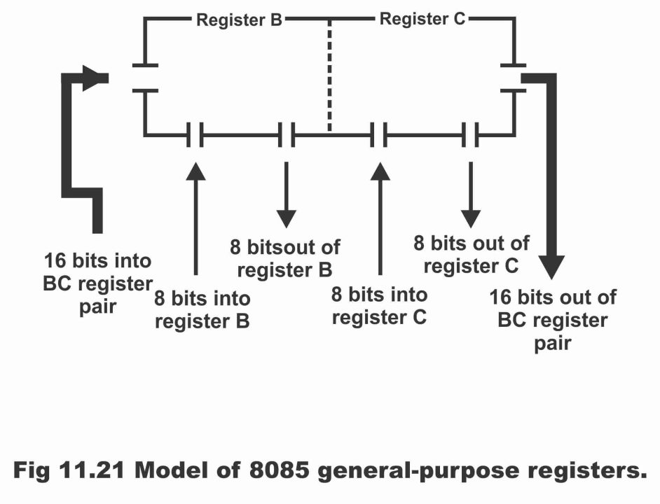
According to this figure, one data bit can enter either B or C and it can also be pulled out. In other words, 16 bits can enter into its pair and can also omitted, because in this situation, register pair act as a 16-bit register. Three sets of pairs of these general-purpose registers exist in a 8085 model (i.e. BC pair, DE pair and HL pair). The word B, C, D and E represents every register, whereas word H and L indicate high and low. HL register pair is generally used for different types of objectives as compared to other pairs.
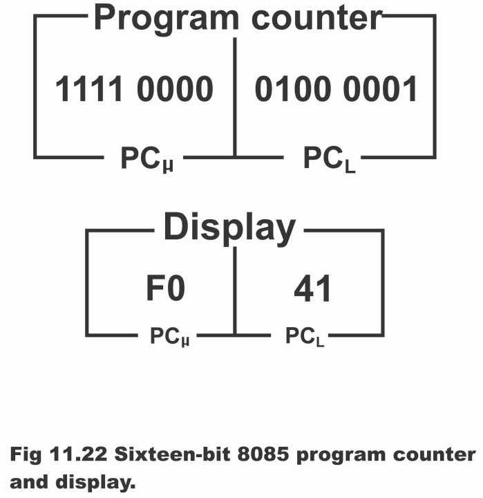
Program Counter
An 8085 microprocessor chip consists of 16 – bit program counters (operation details of which have been mentioned in microprocessor architecture). This program counter has been divided into two parts during some of the operations. Its upper byte or 8 – bits, is called PCH (for high program counter) and lower byte PCL (for low program counter).
As such, program counter operates as a 16 – bit counter. However, sometimes (particularly when subroutines are included) it is considered necessary use by means of dividing into 2 bytes (or two 8 – bits parts). Remember that display of a program counter is in a 4 hexadecimal digits form.
Remember that subroutines (which are also known as sub–programs) are programs, which have been written in such a manner that whenever they are required to be used with other programs, they can be used without rewriting. In other words, subroutine is a standard program which has been written in such a fashion, that whenever needed, it can be used as a part of some other program.
Figure 11.22 – 16 – bit 8085 program counter and display
Index Registes
Just like 8080, no index register exists on 8085 as well.
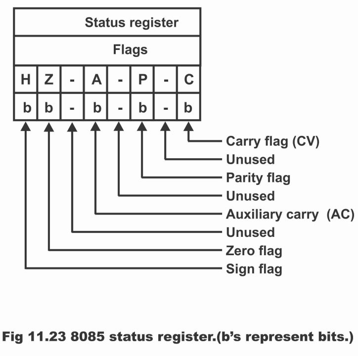
Status Register
8085 consists of such status registers, each of which 8 – bit register has 5 flags as has been illustrated in figure 11.23
Parity flag deals with the topic or subject which has not yet been brought up for discussion. Parity in fact describes 1s existing in a binary number. Parity can either be even or odd. When 1s in any binary number are even, or the number of 1s is even, these number reflects the presence of an even parity. For example, a binary number is 0110 0000. As the number 1s in this number is two, therefore it is an even parity. When the number of 1s in any binary number is odd, this number reflects the presence of an odd parity or it is known with reference to an odd parity. For example, a total of three1s exist in a binary number 0111 000 and as 3 is an odd number, therefore this binary number reflects an odd parity. If parity is even, then parity flag becomes set (1) and in case parity is odd, then parity flag becomes clear (0). Error checking and data communication become easy by means of a parity track.
Figure 11.23 – 8085 status register (b’s represent bits)
Stack and Stack pointer
8085 microprocessor consists of a stack along with a 16- bit stack pointer (process of stack and stack pointer has been mentioned in the section of microprocessor structure)
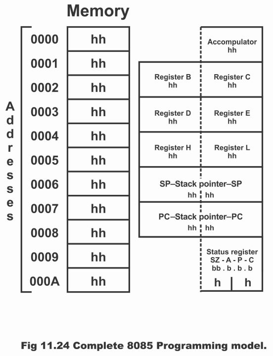
Complete Model
A complete model of 8085 microprocessor has been illustrated in figure 11.24. In this model, six register (which have been denoted as B, C, D, E, H and L) exist apart from addresses, memory and accumulator. These six registers operate separately as 8 – bit register and 16 – bit register, three registers. Moreover, a status register containing 5 flags can also be seen in this model apart from a stack pointer and a program pointer.
Binary and hexadecimal have both been displayed in the status register. Small letters h, s and b, s within it, reflect data existing on each register or memory location. Every “h” means a hexadecimal digit or nibble (which is a collection of 4 bits), whereas every “b” means one bit (1 bit). When we use this model, we put actual values in place of h, s and b, s.
Figure 11.24 – Complete 8085 programming model
For further clarification, a block diagram of an 8085 microprocessor has been illustrated in figure 11.25, which has externally been provided a bidirectional data bus, an address and multiple control lines (here control lines pertinent to bus transfer have only been illustrated). Data bus been denoted by the symbol DBUS and it comprises 8 lines. The information existing on these 8 lines is called byte and this name is used to indicate an 8- bit word. Address bus (which has been indicated by the symbol ABUS) consists of 16 lines. Which is specified for 216 = 64K possible addresses. As such, this, microprocessor is capable of communicating with a 64K memory unit.
Internally, this microprocessor consists of processor registers (B, C, D, E, H), one accumulator register (which has been denoted by A) and a temporary register1. These registers have 8- bit capacity and can store data up to one byte. ALU operates on the basis of data stored on an accumulator and temporary register and transmits outcome obtained as a result of this operation towards A or other six processor registers via internal bus. Status register stores status bits (e.g. from ALU to end carry), sign–bit value and zero result induction for further analysis (remember that status bit conditions are also sometimes known as conduction code bits or flag bits). The operation code of any instruction passes on to instruction register (IR), where this code decodes and informs about the necessity of micro operations’ sequence in order to execute the operation. Timing and control units supervise all internal operations taking place within a CPU and external control lines in a micro–processor.
Figure 11.25 – Block diagram of microprocessor
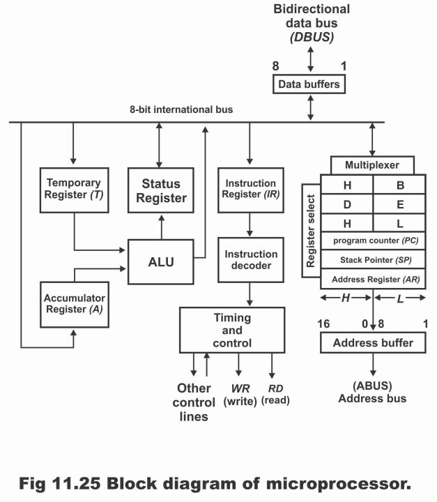
Address buffers fetches information via main sources i.e. program counter (PC), stack pointer (SP) and address register (AR) transmits it on address bus (ABUS), as has been illustrated through the figure. The address bus also fetches address information from a pair of processor registers. Three pairs of processor registers (i.e. BC, DE and HL) can provide a 16 – bit address. Every processor register comprises 8 bits and when an extra register is combined with it, it forms a 16 – bit register pair. Here, symbol H reflects 8 high order bits (i.e. 9 to 16) and symbol L reflects low order bits (i.e. 1 to 8).
Previous Topic: Microprocessor Architecture / Organization in Digital Electronics
Next Topic: How to design digital clock using counters decoders and displays
Discover more from Electronic Clinic
Subscribe to get the latest posts sent to your email.