555 Timer as an Astable and Monostable Multi-Vibrator with circuit diagram
Last Updated on August 5, 2025 by Engr. Shahzada Fahad
Table of Contents
Types of Timer
According to function or operation, types of a 555 timer are as under:
(1). 555 Timer as an Astable Multi-vibrator
(2). 555 Timer as a Monostable Multi-vibrator
Astable Operation of 555 Timer
We know that a-stable is a digital timing circuit, which can be connected as an astable Multi-vibrator (remember that astable means having two states, however neither of these two states is stable). In figure 6.9, this timer has been depicted being applied as an astable Multi-vibrator. In fact, a 555 timer is basically a switching circuit with two specific output levels. If external components are connected with this timer in a proper manner (as has been portrayed in the figure) none of its output level remains stable (that’s both of its levels tend to become an astable or unstable). As a result, this circuit moves unceasingly back and forth between these two unstable states. In other words, circuit tends to oscillate and a periodic rectangular type waveform (known as clock waveform) is obtained via it. As none of its output state is stable, therefore, this circuit is called astable. And is often known as free-running non-sinusoidal oscillator or free -running Multi-vibrator or astable Multi-vibrator. The oscillation frequency and duty cycle of this circuit is accurately controlled by means of two extrinsic resistors and a single timing capacitor.
Figure 6.9 -A 555 timer connected as an astable Multi-vibrator
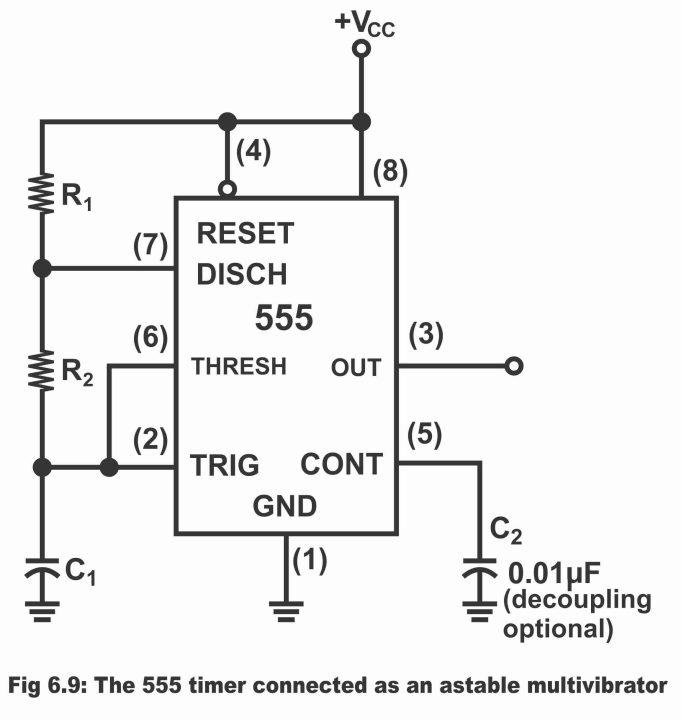
If an astable Multi-vibrator shown in the figure is cautiously observed, it becomes obvious that threshold input (THRESH) has been connected here with trigger input (TRIG) i.e. pin number 6 is being short with pin number 2. The external components existing on this circuit are two resistors R1 and R2 and one capacitor C1, which form a timing network, through the help of which oscillation frequency of the circuit is set (i.e. by means of changing the values of R1, R2 and C1, while staying within definite limits, oscillation frequency of a circuit can be changed as desired. Here, another capacitor of 0.01 micro Farad C2 has been connected to control input (CONT) which is meant for the purpose of decoupling or noise immunity and it does not cast any sort of impact on the circuit operation. Under certain circumstances, this capacitor can be turned off.
Astable Multi-vibrator Operation
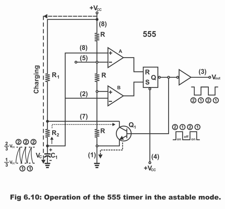
Primarily, when a power supply is turned on, in this situation capacitor C1 is uncharged and thus, the value of trigger voltage (pin 2) is zero volt. As a consequence, comparator B’s (with which trigger input has been connected) output will be high and comparator A’s output will be low. Comparator B’s high output transmits on RS latch due to which the latch sets (set means 1) however, a low output results from it (see bubble sign above the latch output). Thus, discharging transistor Q1 turns off (because transistor base has directly been connected to RS latch output, due to which voltage level of both tends to be the same). As a result of Q1 being turned off, capacitor C1 starts charging via resistors R1 and R2, because charging action starts as soon as Q1 turns off. This has been illustrated in figure 6.10. When capacitors’ voltage value reaches up to 1/3VCC, comparator B output turns out to be low and when capacitor voltage reaches 2/3VCC, comparator A output becomes high (absolutely opponent to the above -mentioned states). The high output of comparator A is transmitted on RS flip-flop, resultantly flip-flop resets (because comparator A output is directly linked with RS flip-flop’s R input, as has been illustrated vide figure). As soon as flip-flop resets (reset means zero), its output becomes high. Thus, base of transistor Q1 also becomes high, due to which transistor turns on. As soon as discharging transistor Q1 turns on, capacitor C1 starts to discharge via resistor R2, as has been illustrated via an arrow sign in the figure. With the discharge of capacitor, comparator A turns out to be low. The point where voltage value equals to 1/3VCC as a result of capacitor’s continual discharge, timer triggers automatically at that point. As such a new charging cycle kick-off. As timer triggers, comparator B turns high, hence latch sets. As a result, transistor turns off owing to a low Q1 base and capacitor C1 starts re-charging. Thus, as a result of an inception of a new charging cycle, all afore-mentioned operation repeats once again. Consequently, a rectangular type wave is received on output, the duty cycle of which depends on the values of R1 and R2. (i.e. duty cycle of output can be adjusted by means of changing values of R1 and R2). Oscillation frequency or output waveform frequency can be determined with the help of following formula:
f = 1.44 / (R1 + 2R2) C1
As C1 charges via R1 and R2 (through selecting an accurate value of which, output duty cycle can be set), but discharges only via R2, therefore if R2 value is turned quite high or doubled as compared to R1 value (i.e. R2>>R1) the 50 % minimum duty cycle value can be achieved. As charging as well as discharging timers almost become equal.
Figure 6.10-operation of a 555 timer in an astable mode
The method for determining duty cycle in case of an astable Multi-vibrator, is as below:
(i). Charging Time: When output is high, C1 requires following time for charging from 1/3 VCC to 2/3 VCC
tH = 0.7 (R1 + R2) C1 here, 0.7 is time constant of capacitor
(ii). Discharge time; When output is low, the time which C1 requires from 2/3 VCC to 1/3 VCC for discharge, its value can be ascertained with the help of following formula;
tL = 0.7 R2 C1
(iii). Time Period of Output Waveform; Time period (T) of output waveform is the sum of charging and discharging time, formula of which is as below;
T = tH + tL = 0.7 (R1 + 2R2) C1 … (1)
We know that time period is inverse to oscillation frequency i.e.
f= 1/T = 1.44 / (R1 + 2R2) C1 … (2)
(iv). Duty Cycle; The ratio between charging time tH and time period T (or an output waveform’s full cycle time) is called duty cycle. i.e.
Duty cycle = tH/T = tH / tH + tL = 0.7 (R1 + R2) C1 / 0.7 (R1 2R2) C1
Remember that duty cycle is always expressed as percentage.
Duty cycle = [R1 + R2/ R1 + 2R2] 100%
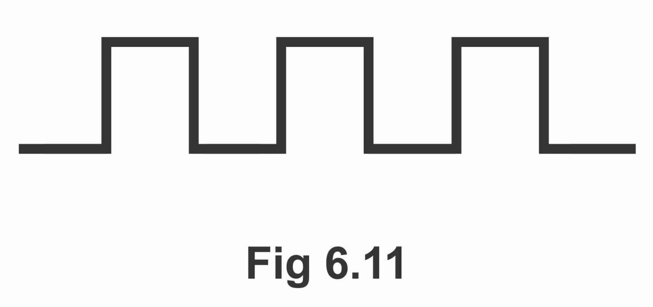
It must be kept in mind that output of an astable 555 Multi-vibrator may either be symmetrical or asymmetrical. When both charging as well as discharging time of a capacitor are equal (i.e. tH = tL), under such a situation, symmetrical or equivalent output waveform is obtained. This has been illustrated via figure 6.11. The duty cycle of a symmetrical waveform is 50% i.e. its output remains 50% on while 50% off. In other words, 50% of output waveform builds up on top portion while 50% on the bottom segment. As a result, a square type output wave is obtained.
Figure 6.11
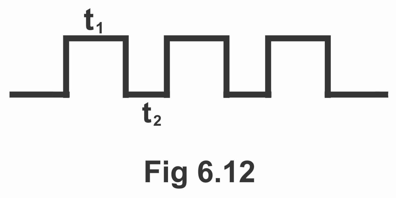
If charging and discharging time of the capacitor are not equal (i.e. tH tL), in such a situation asymmetrical waveform results (i.e. a rectangular type waveform instead of a square one), as has been illustrated vide figure 6.12. This type of waveform is always expressed with relation to a duty cycle. For example, if duty cycle is 0.45 (or 45%), it means that signal remains on ground (GND) for 45% of the overall time (i.e. remains on low level) whereas remains on high level for 55% of overall time. As a result, a rectangular shaped or asymmetrical output waveform is received.
Figure 6.12
If duty cycle is required to be reduced than 50%, a slight modification is made within the circuit. According to which C1 only charges via R1 and discharges via R2 (this can be possible only by means of installing a diode parallel to R2). When duty cycle is required to be reduced than 50%, R1 is reduced with respect to R2. In such a situation, formula of duty cycle turns out to be as follows;
Duty Cycle = [R1 / R1 + R2] 100 %
Alternative Explanation of an Astable MV Operation
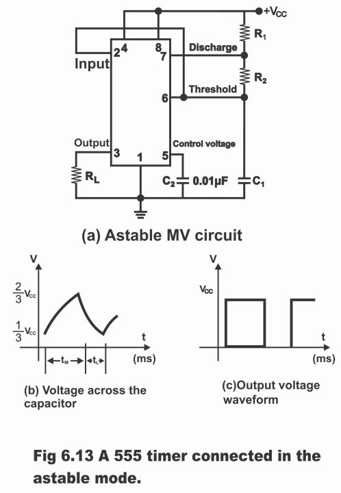
In figure 6.13, a 555 timer has been shown connected in an astable mode, according to which threshold terminal has been connected directly with the input triggered terminal (i.e. pin number 6 is short directly with pin number 2). In this circuit, two resistors R1 and R2 and a capacitor C1 are external components, which form a timing network. A capacitor C2 is also present in this circuit, which has been connected with control voltage. The function of this circuit is just to perform decoupling. The process of circuit’s operation is as under;
(1). As soon as the circuit is energized, then immediately thereafter;
- Voltage level on threshold and input terminal turns out to be low (as compared to 2/3 level of VCC)
- Output is high
- Discharge path (pin number 7) turns open
- Capacitor C1 starts charging with time constant (R1 + R2) C1 till VCC.
(2). When voltage value parallel to capacitor C1, which is also connected to threshold terminal reaches 2/3 VCC (i.e. when capacitor C1 voltage are 2/3 of the control voltage), then comparator sets output on low and the discharge path tends to close.
(3). As a result of closure of discharge path, capacitor C1 discharges very swiftly via R2, in such a situation, discharge time constant is R2C1.
(4). When C1 capacitor discharges up to 1/3 level of VCC, the comparator circuit tends to push output high, further discharge path also opens.
(5). C tends to re-charge via (R1 + R2) C1 time constant up to VCC
(6). After this, afore-mentioned 2, 3, 4 and 5 steps are repeated alternately until the circuit has been de- energized (i.e. until the circuits’ supply is turned off, above-mentioned factors are repeated continuously)
As a result of operation of an astable circuit as shown in figure (a), voltage waveform received parallel to capacitor has been shown in figure (b) and output voltage waveform received on output has been illustrated via figure (c).
Figure 6.13-A 555 timer connected in an astable mode
Monostable or One-Shot Operation of 555 Timer
A 555 timer can also be used as a monostable Multi-vibrator. A monostable Multi-vibrator is such a switching circuit, which has a stable state as well as a semi-stable state. If a slight modification is made on the outer wiring of 555 timer circuit (or various components are fitted around 555 timer), a monostable circuit will be fabricated, which is immensely being used in industry for different timing applications. This circuit encased in an IC, is just analogous to a basic 555 timer circuit, with the only exception that in monostable circuit, two capacitors and a resistor do also exist outside IC. According to the normal operational mechanism of a monostable circuit, when it is triggered towards semi-stable state (because under its normal state, this circuit persists on its stable state) it remains in its semi-stable state until a pre- determined given period of time. After this specific period of time, the circuit switches back to its stable state. The circuit survives on a stable state until some alternative trigger is received on it. As this circuit has just one stable state, therefore it is called monostable Multi-vibrator, or just monostable or monostable switching circuit or one-shot.
The standard logic symbol of a monostable has been shown in figure 6. 14 (a). Here, input has been denoted as TRIGGER whereas output has been represented by Q, while the complement of Q output in this symbol has been represented by Q. Input trigger circuit can be made sensitive for either positive transition (PT) or negative transition (NT). In this situation, it is called negative edge triggered (i.e. here we will talk about the circuit operation from perspective of negative edge triggered). According to which, when the circuit is in its stable state, at that its output Q is zero or low. This can be seen in terms of waveforms as shown in figure (b). According to figure, once the circuit triggers, Q turns high or becomes 1. After remaining high on 1 for some specific period of time “t”, it retreats back to its stable state i.e. 0, until another NT appears on the trigger input.
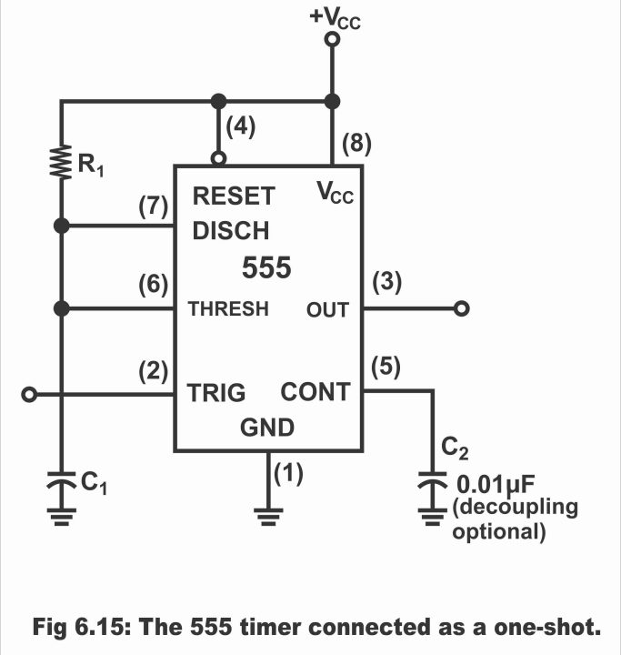
In figure 6.15, a 555 timer has been illustrated connected as a one-shot or monostable multi-vibrator circuit. In this figure, one external resistor R1 and two capacitors C1 and C2 can be seen planted outside an IC. Here, control voltage input (CONT) has not been applied and it has been connected with a decoupling capacitor C2, so that noise signals could be blocked from casting any sort of unpleasant influence on trigger and threshold levels. However, without C2 too, performance of this timer is quite satisfactory. As C1 capacitor occupies less space, and its price is also low, therefore it has continued to be included in the circuit generally. The value of this capacitor normally happens to be 0.01 micro Farad.
Figure 6.15-A 555 timer connected as a one-shot
Monostable Multi-vibrator Operation
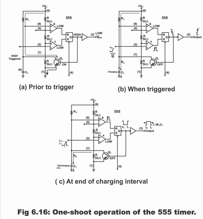
As long as a monostable timer is not provided a trigger pulse, its output remains low or zero and discharge transistor Q1 also remains on. As a result of an “on” Q1, capacitor C1 keeps discharging. This has been illustrated via figure 6.16 (a).
When a negative edge trigger pulse is applied on circuit’s trigger input, output turns out to be high and discharge transistor also turns off. As a result, capacitor C1 start charging till VCC via resistor R1. This has been illustrated vide figure (b).
When capacitor C1 charges up to 2/3 VCC, circuit returns back on its stable state and output turns low once again. As a result of output turning out to be low, transistor Q1 also turns on immediately and capacitor C1 starts discharging. The circuit sustain on this state until some other pulse is received on trigger input. Remember that width of output pulse is determined through R1 and C1 time constant via following formula.
tw= 1.1 R1 C1
Figure 6.16-one shot operation of a 555 timer
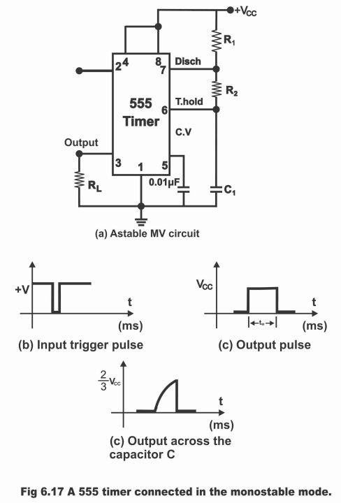
For further explanation, a 555 timer has been shown connected in a monostable mode in figure 6.17. At the same time, its operation has also been illustrated in the shape of waveforms. Further elaboration about working of this circuit can be done in the following manner;
(1). When circuit is energized, then
- its output is low
- No charge exists on capacitor C1
- Discharge circuit (pin number 7) tends to be closed
(2). When a negative going trigger input pulse is provided, as has been illustrated vide figure (b), output tends to become high and discharge path also turns open.
(3). Capacitor C1 charges till VCC with time constant R1 C1
(4). When capacitor voltage VCC reach up to 2/3 level of control voltage, then comparator sets output on low and discharge path closes again
(5). As the discharge path closes, capacitor C1 starts to discharge very speedily. Waveform appearing on trigger input has been denoted in figure (b) output pulse in figure (c) and shape of waveform appearing parallel to capacitor has been depicted vide figure (d).
Figure 6.17-A 555 timer connected in monostable mode
Applications of Clocks & Timers
Clocks and timers are used in digital circuits for the following different purposes.
(1). Clock pulses are used in order to operate a flip-flop
(2). They are used in different oscillator circuits for producing desired frequencies
(3). Periodic square waves obtained from clocks are used in digital systems as synchronizing signal
(4). Clocks and timers play a very crucial role in different computer operations
(5). They also play a pivotal role in frequency counters
Previous Topic: Types of Multi-vibrator: Astable, Monostable and Bistable Vibrator
Next Topic: Shift Register: Shift Right and Shift Left Registers with circuit diagram
For electronics and programming-related projects visit my YouTube channel.
Discover more from Electronic Clinic
Subscribe to get the latest posts sent to your email.