Shift Register: Shift Right and Shift Left Registers with circuit diagram
Last Updated on December 1, 2022 by Engr. Shahzada Fahad
Introduction
A group of flip-flops which is used for storing or protecting a binary number or binary data, is called register. In other words, a register is such a group (collection) of memory elements in which ordinary memory elements or flip-flops, work collectively as a unit. The function of a register is just to store a binary word. In other words, a register is a device, which performs the task of storing information and flip-flops are used for its manufacturing process. As every flip-flop existing on the register can store just one binary bit (0 or 1) of information at a time, therefore in order to store “n” bits in a register, “n” flip-flops are required (i.e. the number of bits which are desired to be stored on a register, same number of flips-flops are used on it according to the number of bits). For example, if an 8- bit word or binary number is desired to be stored in register, a total of 8 flip-flops are required to be used in this register. As a flip-flop can store just one bit at a time, the total number of bits in a register or range of bits is called storage capacity of that register.
A shift register is a group of flip-flops, wherein all flip-flops have been inter-connected in such a manner that a binary number can be shifted both inside or outside these flip-flops. In other words, a group of inter-connected flip-flops, on which binary number or binary information can be shifted both inside or outside of these flip-flops, is called shift register. A shift register is also a storage device, wherein binary data or digital information is stored. This device is designed in such a manner that its stored bits can be shifted or transmitted from one flip-flop to another flip-flop (i.e. shift registers are used for storing and shifting of data (0 and 1) in a digital system). Thus, a shift register is a kind of digital circuit, which performs two basic functions i.e. data storing and data shifting. Remember that shift registers are a form of sequential logic circuits, which are being extensively used.
The storing capacity of a register or its capacity to store data refers to the number of digital data bits (0 and 1) which it can store or retain inside it. As every stage of a flip-flop present in the shift register reflects storage capacity of a bit (that is every flip-flop of all the flip-flops existing on a register can store just one bit) therefore, the number of stages (flip-flops) in a register represents its overall storing capacity. However, capacity of a register to shift data from one flip-flop to another flip-flop or from one stage to other stage existing within it, or capacity of a register to let data enter into it or let data to be ejected out of it, depends on the use of clock pulses.
In short, a shift register is constructed through binary storage elements (i.e. flip-flops) which are wired or cascaded together in a manner that a bit stored on one element can be shifted to the adjacent element (if flip-flops are connected together in such a way that output of one flip-flop is input for other flip-flop, this process is called cascading of flip-flops). However, it has to be remembered that all storage registers present in a digital system can be made to operate together via an input clock pulse or shift pulse. Therefore, when a shift pulse is applied, then as per needs, data present on shift register can shift only to one-bit position at a time in a serial manner right or leftward. As a result of this shifting or moving feature just one-bit data at a time, shift registers are widely used for carrying out functions like counting, frequency dividing or arithmetic operations etc.
The shifting mechanism in a shift register can also be understood by means of a calculator display screen, in which as we press digits on a keyboard, number present on calculator’s display keep shifting towards left and first digits on the display also do not disappear (because shift register within a calculator also operate both as a memory as well as shifting element). For example, in order to enter 268 number in a calculator first of all number 2 key is pressed momentarily and then released. In this way, number 2 will appear on right side of the calculator’s display. After this number 6 key is pressed and then released. As soon as 6 is pressed, number 2 (which was primarily towards the right most side of the screen) shifts one position towards the left and its place is taken by number 6. Thus, number 26 displays on calculator screen. Finally, we have to press and release number 8 key on the calculators’ keyboard. As a result, number 2 and 6 shifts further by one position towards left and thus, number 6 is replaced by 8. As such, number 268 starts displaying on the calculator’s screen. From this example, both features of shift registers i.e. temporary memory and shifting have been manifested, by means of which shift register has assumed the status of an extremely invaluable device within multiple digital systems.
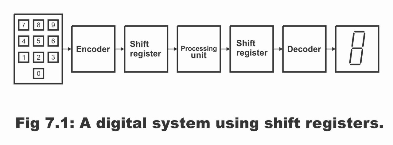
In figure 7.1, the usage of a shift register has been demonstrated in a digital system (calculator or computer), wherein a shift register fitted prior to a decoder and after an encoder, has been shown. Here, register mounted after the encoder, temporarily stores information for a processing unit and register fixed between processing unit and decoder, temporarily stores information communicated between these two. It must be remembered that a shift register can be applied in a number of other places as well within a digital system.
Figure 7.1- a digital system using shift registers
Shift Right and Shift Left Registers
We know that when a clock pulse is applied on a basic shift register, then according to “one-bit position per clock pulse” principle, data stored on the register shifts in a serial manner from right to left. Thus, serial shift registers are of the following two types according to its operation.
(1). Shift right register
(2). Shift left register
Shift Right Registers
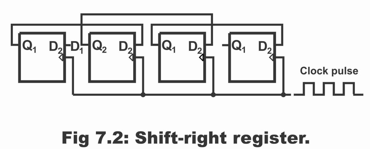
Shift registers wherein input enters from left side and numbers already present on it, effuse or excrete from right side, are called shift right registers. In other words, registers which transfers or shifts input data rightwards, are called shift right registers. In figure 7.2, a shift right register has been illustrated, which contains four flip-flops (it means that this register can store only a 4 – bits binary number). According to this figure, every Q output keeps on setting D input of every next flip-flop. When rising clock edge arrives, then stored bits shift rightward according to the “one–bit position per clock pulse” principle. For example, Din value is 1 (i.e. Din = 1) and Q = 0000, then upon influx of the first positive clock edge (i.e. clock pulse), leftward flip-flop tends to set. In such a situation, all data inputs except input on the left side, are 0s. Thus, as a result of flip-flop D3 being set, the word stored within a register is as follows;
Q = 1 0 0 0
With the appearance of this word, values of D2 and D3 turn out 1 (i.e. D2 = D3 = 1s), because Q3 output tends to set output D3 (see figure). Similarly, following results with the advent of second rising clock edge.
Q = 1 1 0 0
Similarly, following changes take place as a result of 3rd clock pulse and 4th clock pulse.
Q = 1 1 1 0
Q = 1 1 1 1
Fig7.2
For further clarification, operation of a shift right register has been illustrated in figure 7.3. This shift register also comprises four binary storage elements (i.e. four flip-flops) and number 1011 is pre-stored on it. A binary number 0110 exists on the serial outside this shift register, which is desired to be stored in this register. As clock or shift pulses are applied on the register, then according to one-bit position per class pulse principle, stored digits in shift register disappear after exuding one by one from the right end. And at the same time, outer digits present on the left, keep on shifting to register one by one.
Figure 7.3 – operation of shift register
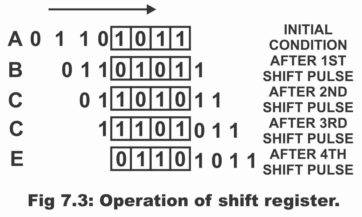
In figure (A) initial state of a shift register has been depicted. According to figure (B), after the advent of first clock pulse, already stored numbers in the register, as per one–bit position shift rightward from its place. Thus, most rightward lying bit (1) in shift register, shifts or transfer out of the register and rightward lying first bit (0) of the external number, moves to the leftmost space of the shift register (remember that as a result of each shift pulse, all inputs present within a shift register shift one position towards right. Thus, empty space which is created towards left of the register, an external bit is inserted on it).
Similarly, after the arrival of second shift pulse (as has been shown in figure C), the most rightward lying bit of the shift register, shifts out of the register. Whereas the most rightward lying next bit present outside register, enters the most leftward lying empty space of the register. As such, similar kind of situation repeats with the arrival of third shift pulse and fourth shift pulse (as can be seen via figure D and E). Hence, after four shift pulses, the pre-stored number in the register, disappears after completely shifting out of the register while the external number on left end of the register, completely shifts from outside and stores on the register after four shift pulses. It remains in it until some other external number is applied on register’s input after the entrance of a new shift pulse.
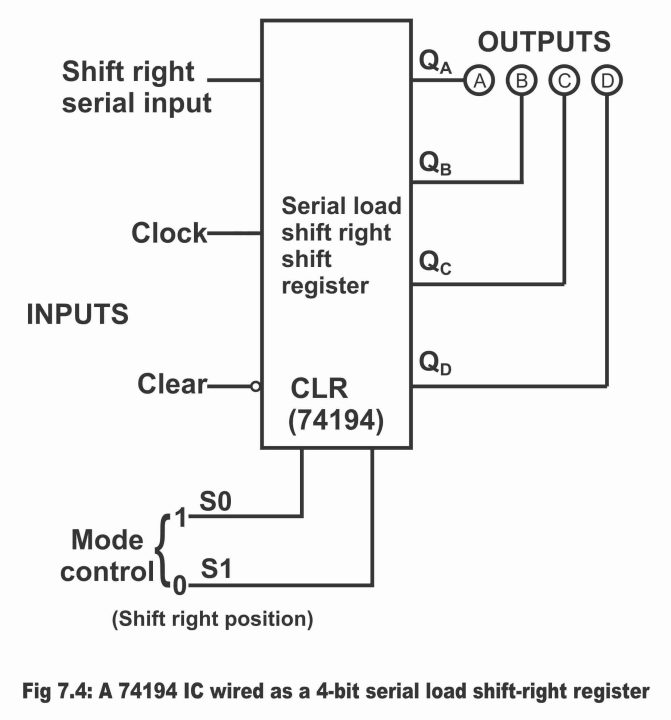
In figure 7.4, a serial load shift right register has been demonstrated, which is of 74194 – IC type. As this 74194 – IC register is a universal shift register, therefore when it is used as a shift right register, its mode control (S0, S1) should be on shift right position according to the picture (i.e. S0 must be on 1 whereas S1 on 0). Here, rightward shifting actually means shifting from QA to QD. that’s this register shifts data towards right and data extricating from QD gets disappeared or lost.
Figure 7.4 – 74149 – IC wired as a 4 – bit serial load shift – right register
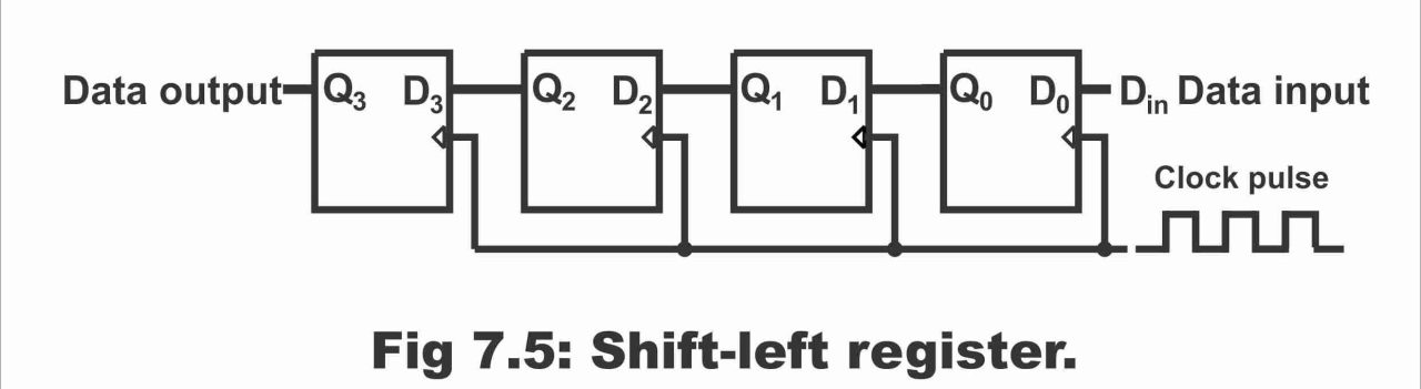
Shift Left Registers
A shift register, wherein input data is entered from the right side, whereas digits already present on the register leave out/ remove from the left side, are called shift left registers. In other words, registers which shift input data towards left, are called shift left registers.
In figure 7.5, a shift left register has been elucidated, which consists of four D type flip-flops. According to the figure, Din sets the right most flip-flop, Q0 sets the second flip-flop, Q1 sets third flip-flop and Q2 sets fourth or final flip-flop. Remember that every time this register receives next positive clock pulse its stored bits shift leftwards as per one position / clock pulse principle. For example, if a state of Din = 1 and Q = 0000 exits on register, in such a situation, the rightmost flip-flop (Q0) sets with the arrival of first clock pulse (or rising clock edge), as a result values of all data inputs are 0, except 1 existing on the right end. In other words, stored word in the register is as follows;
Q = 0 0 0 0
As first flip-flop’s output (Q0) located on right end, is input of the second flip-flop (i.e. D1 = D0), thus D1 value is 1 or equal to the value of D0. Therefore, as a result of collision of next clock pulse, Q1 flip-flop gets set and stored number in the register turns out to be as follows;
Q = 0 0 1 1
Similarly, as a result of third and fourth positive clock pulses, following changes take place in the register;
Q = 0 1 1 1
Q = 1 1 1 1
Similarly, after four shift pulses, already existing number on the register shifts out completely from the register and turn lost or disappear. And external number on right end of the register completely gets shifted and stored in the register after four shift pulses. It remains in the register so long as the value of Din is 1 (i.e. Din = 1) or as long as change does not occur in Din.
Figure 7.5 – shift – left register
Suppose that Din value has now been changed to 0 (i.e. Din = 0). Thus, in such a situation, continuous clock pulses cause following changes in the register;
Q = 1 1 1 0
Q = 1 1 0 0
Q = 1 0 0 0
Q = 0 0 0 0
It must be remembered that as long as binary value of Din is 0 (i.e. Din = 0) no change occurs in the stored register numbers even in the presence of insistent clock pulses.
The function of shift left register has further been elaborated with the help of its simple manifestation vide figure 7.6. this register consists on four binary storage elements and binary number 0000 is pre – stored on it. This can be seen in figure “A” via its primitive state. Whereas, binary number 1111 is desired to be stored on the register. On the arrival of first clock pulse, all bits of pre–stored numbers in the register shift towards left according to one – bit position. As such, one bit moves out from left end of the register and is lost. And most rightward bit of the external bits present on right side of the register, shifts inside the register, as has been illustrated vide figure B.
Figure 7.6 – operation of shift left register
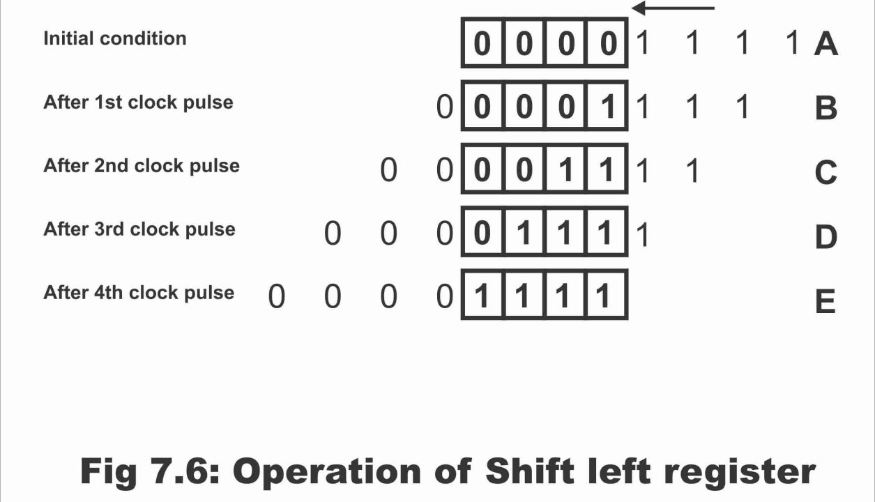
Exactly similarly, on receiving the next clock pulse, bits on left side of the register leave or quit one by one and vacant space on the right side of the register, all external number bits enter and stored on the register turn by turn. It must be remembered that movement or shifting direction of external bits which entered register, has to be from right to left according to one–bit position. This has been shown via an arrow sign above figure. Therefore, this type of register is called shift–left register.
a serial load shift – left register has been depicted, which is available inn 74194 – IC shape. Remember that when this IC is required to be operated as a shift-left register, its mode control must be on the shift-left position according to the figure (i.e. S0 should be on 0 and S1 on 1). In such type of register, data intrudes with each clock pulse via D or QD and tends to shift towards A or QA.
Previous Topic: 555 Timer as an Astable and Monostable Multi-Vibrator with circuit diagram
Next Topic: Different Types of Shift Registers In Digital Electronics
For electronics and programming-related projects visit my YouTube channel.
Discover more from Electronic Clinic
Subscribe to get the latest posts sent to your email.
Hi, thanks for explanation but in fig 7.3. there is a typo, you need to change ABCCE to ABCDE. Otherwise very clear. If you left shift 16 bits into a 12 bit register, you lose four LSBs – in other words you lose some accuracy, is that correct?