Different Types of Shift Registers In Digital Electronics
Last Updated on December 1, 2022 by Engr. Shahzada Fahad
Table of Contents
Types of Shift Registers
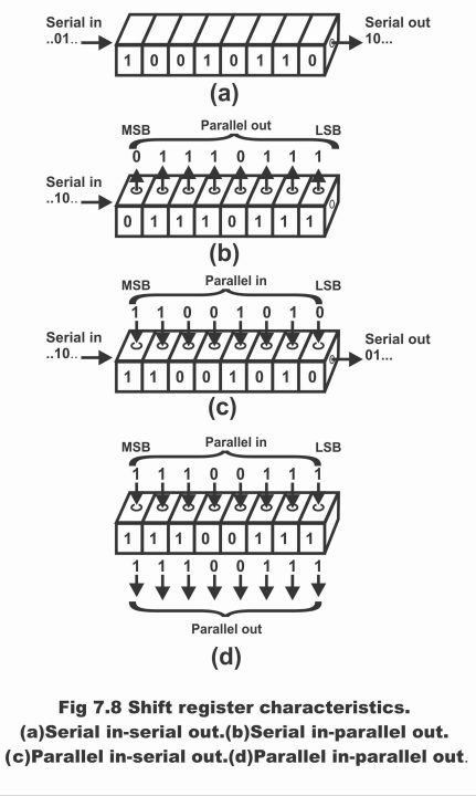
All bits existing in a binary number or binary data can be shifted from one spot to another by means of two methods. According to the first method, data is shifted in a serial form at a time via one-bit method. This method is called serial shifting. In the second method, all data bits are transferred or shifted at a time in a parallel form. This method of data shifting is called parallel shifting. As such, there are two methods for shifting in a data to a register (serial or parallel), similarly there are two methods for shifting out data from a register as well. Therefore, four types of shift registers on the basis of shifting data to a register, are as follows;
(1). Serial in-serial out
(2). Serial in-parallel out
(3). Parallel in-serial out
(4). Parallel in-parallel out
It has to be remembered that afore-mentioned types are commonly available as commercial TTL MSI/LSI circuits. In figure 7.8, basic concept of these types of registers has been illustrated for an 8-bit register. Explanation of above-mentioned types is as follows;
Figure 7.8-shift register characteristics (a). Serial in- serial out (b). Serial in- parallel out (c). Parallel in-serial out (d). Parallel in-parallel out
Serial in-serial out Shift Register
Serial in-serial out (which is briefly denoted as SISO) is a shift register which receives data in serial form and also transmits its stored information on output in a serial form (i.e. this type of register receives just one bit (0 or 1) at a time on a single input line) and at the same time, also produces an output bit at a time in serial form). In other words, a register which receives data on its input in a serial form and also provides data from its output in serial form, is known as Serial in- serial out shift register.
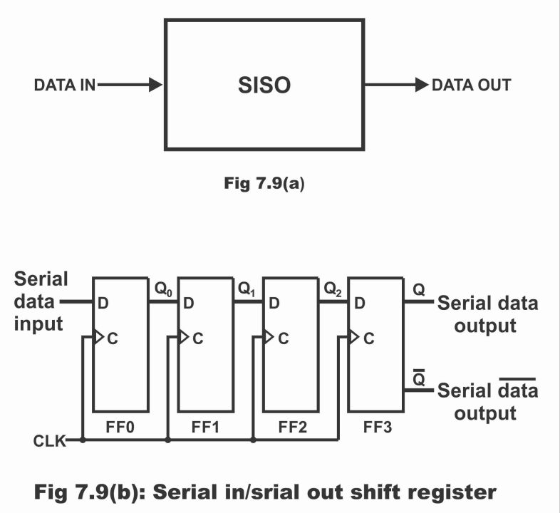
In figure 7.9 (a) symbol and shape of Serial in- serial out shift register and in figure (b) design and hardware of a four-bit serial in-serial shift register has been shown, which consists of four D flip-flops (remember that apart from D flip-flop, clocked RS flip-flop and JK flip-flops can also be used for construction of shift register). This four-stage shift register can store just 4-bit data (i.e. storage capacity of this register is 4-bit). However, besides 4-bit size, shift registers are also available in 5- and 8-bit sizes. In figure (b) D type flip-flops have been inter-connected in a manner that all the flip-flops clocks have been shorted together. Moreover, output of FF0 flip-flop has been recombined with FF1 flip-flop. Similarly, FF1 output has been provided to FF2 and FF2 output to FF3 flip-flops. On data input D of this register, first of all serial input data is provided and output is received from serial data output line Q3.
Figure 7.9 (b)-Serial in- serial out shift register
Suppose that we want to store or shift data consisting of four bits (1010). For this purpose, first of all binary 0 on the data input line is provided. When first clock pulse is received, then first bit (i.e. 0) is stored in flip-flop FF0. In such a situation, states of all four outputs will be as follows;
Q0 Q1 Q2 Q3
0 0 0 0
After this, 1 is received on data input line. After providing 2nd clock pulse, Q0 bit (i.e. 0) shifts one step rightwards, whereas data existing on the input line (i.e. 1), is stored in FF0. Under such a situation, following states emerge on all four outputs;
Q0 Q1 Q2 Q3
1 0 0 0
Similarly, when 3rd data bit (i.e. 0) exists on data input line, then before the advent of the third clock pulse, both stored bits (i.e. 0 and 1) shift one step rightward, whereas 3rd input stores in FF0. In such a situation, out turns out to be as under;
Q0 Q1 Q2 Q3
0 1 0 0
After this, we get last or 4th bit (i.e. 1) on data input line. And as 4th clock pulse strikes, first three bits stored in the register (i.e. 0, 1 and 0) shift rightward one step each, whereas 4th input (i.e. 1) stores in FFO. Resultantly, standard of all four flip-flops becomes as follows;
Q0 Q1 Q2 Q3
1 0 1 0
Thus, in this way entire input data consisting of four bits completely enters or register into shift register in a serial form, where it can be stored any time. If expulsion or shifting of data is ever required from this register, it is shifted outward via Q3output from the register in a serial form. The mechanism for extracting data from register is as below;
When we apply 5th clock pulse, bit existing on Q3 output shifts out from the register and bits present on Q0, Q1 and Q2 move one step ahead (i.e. move ahead rightward by one step). In such a situation, following states prevail on outputs;
Q0 Q1 Q2 Q3
1 0 1
Similarly, when 6th clock pulse is received, data present in the register shifts one step further rightward and bit existing on Q3 output shifts out from register in a serial form. In such a situation, outputs will be as follows;
Q0 Q1 Q2 Q3
1 0
When 7th clock pulse strikes, data present in the register shifts rightward one step further, as a result bit existing on Q3 output shifts out from the register in serial form. In such a situation, flip-flops outputs will be as follow;
Q0 Q1 Q2 Q3
1
When 8th clock pulse strikes, bit existing on Q3 also shift outward from the register in a serial form, as result of which outputs of all flip-flops tend to reset (i.e. all outputs return on their primitive state). in this manner, process of Serial in- serial out is accomplished. In order to understand afore-mentioned detail in a simple manner, an entry of a 4-bit number 1010 into the register has been shown in figure 7.10.
Figure 7.10-four bits (1010) being entered into the register
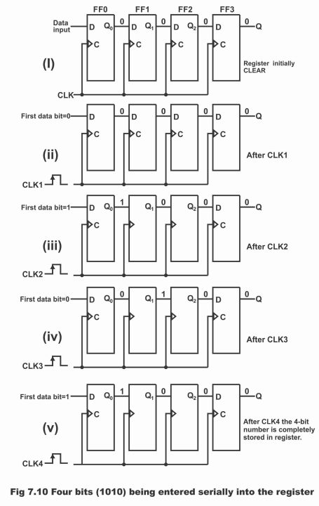
When first bit (i.e.0) strikes data input line D, value of FF0 flip-flop’ s D input turns out 0 (i.e. D = 0 for FF0). When first clock pulse is applied, FF0 resets and 0 bit is stored within it, as has been illustrated in part (ii) of this figure.
After this, 2nd bit (i.e. 1) is applied on data input, as a result D value for FF0 becomes 1 (i.e. D = 1 for FF0), whereas for FF1, D value becomes 0 (i.e. D = 0 for FF1), because D input of FF1 is connected with Q0 output, as has been elaborated vide part (iii) of the figure. When 2nd clock pulse strikes, then 1 existing on data input, shifts to flip flop FF0 (because in such a situation FF0 becomes set) and 0 bit, which previously existed in FF0, now shifts to FF1.
Now 3rd bit (i.e. 0) is applied on data input line and as a result of application of clock pulse, 0 bit enters flip-flop FF0. Bit 1 already stored in flip-flop FF0, shifts to FF1 and already stored 0 bit in FF1, shifts on flip-flop FF2 (i.e. with striking of each clock pulse, all bits stored in the register shift one step rightward in a serial form). This has been elaborated in the fourth (iv) part of the figure.
Now fourth or last bit and pulse is applied on input data, as can be seen in the 5th part (v) of the figure. In such a situation, this input bit 1 enters flip-flop FF0, whereas already stored bit 0 in FF0, shifts to flip-flop FF1. Similarly, stored bit 1 in FF1, shifts on flip-flop FF2 and stored bit 0 in FF2 shifts to FF3. Thus, serial entry of four bits present in the shift register, completes. Remember that these bits remain stored in the register, as long as DC supply is available in flip-flops.
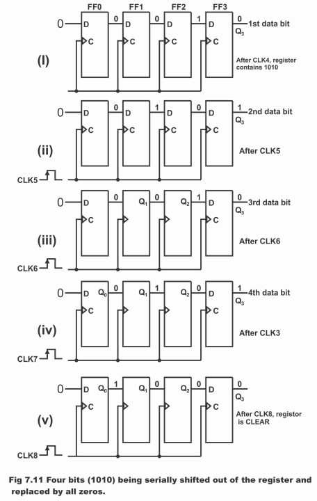
Now, if you want to extricate this data from the shift register, then these bits can be shifted out from register only in a serial form. And bits moving out in a serial manner emit from output Q3 one by one, as has been shown in the figure 7.11.
We know that after application of 4th clock pulse (CLK4), data consisting of four bits (1010) is completely stored in the register and the right most bit of this data (i.e. 0), is received on output Q3, as can be seen in the first part (i) of the figure.
When 5th clock pulse (CLK5) is applied on the register, the 2nd bit (i.e. 1) to the right of data 1010 appears on output Q3, as can be seen in second part (ii) of the figure. Similarly, as a result of applying clock pulse 6 and 7, 3rd bit (i.e. 0) and 4thbit (i.e. 1) shifts on output Q3 alternately. As can be seen in third (iii) and forth (iv) part of the figure. As such, fully stored binary number in the register 1010 shifts out from the shift register’s output in a serial form. However, after 8th clock pulse (CLK8) strikes, shift register gets absolutely cleared, as can be seen in 5th (v) part of the figure. Remember that when all four bits stored in the register are being shifted out, bits of some other number can be stored in the register at that time.
Figure 7.11-four bits (1010) being serially shifted out of the register and replaced by all zeros.
Serial in-parallel out Shift Register
Serial in- parallel out (shortly known as SIPO) shift register is a shift register in which input data bits enter into the register in a serial form (i.e. the right most bits enter first and bits are provided on the register one by one). However, these bits are received from registers’ output in a parallel fashion (i.e. all bits introduced on input are received simultaneously on output in a parallel fashion). In other words, a shift register, which receives data in a serial fashion (in a series of one by one) shifts this data on output in a parallel form (i.e. reflects all output simultaneously), is known as Serial in- parallel out shift register. Remember that contrary to the serial output (in which data output is received as bit by bit on bit by bit basis). As all bits are simultaneously received on output in this shift register, therefore once data has been stored on this register, every bit of the data is available on its corresponding output line. Thus, as compared to Serial in- serial out shift register, which has been discussed above, attribute of this register (i.e. Serial in- parallel out) register is that, as soon as some bit is stored on the shift register, it becomes available on output as well simultaneously (owing to quality of parallel output). Therefore, all bits can be obtained instantaneously from outputs of this type of a register.
In figure 7.12 (a), logic diagram of a 4-bit Serial in- parallel out shift registers and in figure (b) its logic symbol has been displayed. The word SRG4 written inside the symbol means that it is a 4-bit capacity shift register. The operational mechanism of this sort of circuit is as follows;
Figure 7.12-A serial in/ parallel out shift register
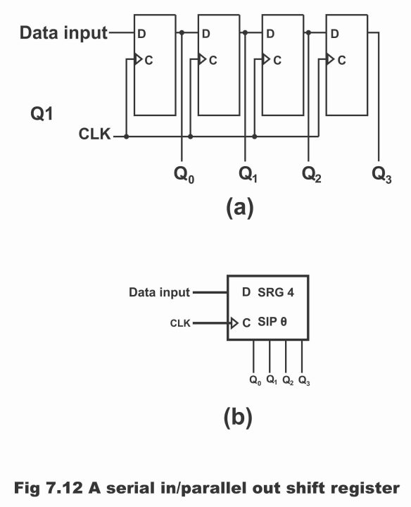
Suppose that we want to store a data comprising four bits 1001 in this register. For this purpose, first of all, the right most bit (i.e. 1) is provided on the data input line. On application of clock pulse, this bit transfers or shifts on output Q0. As Q0 output is also connected with the next flip-flop’s data input D, therefore this output may also be considered as an input of the next flip-flop.
After this, next bit (i.e. 0) is applied on the next flip-flop’s data input line, which as a result of arrival of the next clock pulse, shifts on Q0 output of the flip-flop. However, it has to be reminded here that as a result of advent of this flip-flop, already stored bit on Q0 output, now shift on output Q1 of the 2nd flip-flop. Similarly, with the receiving of next two bits (i.e. 0 and 1) on flip-flop’s data input, clock pulses shift them one step further towards right. And already stored bits in the register, further shift rightward in a serial fashion, as a result of which following state develops on output;
Q0 Q1 Q2 Q3
1 0 0 1
As all these bits shift from input to output in a serial manner, and during the shifting process these bits simultaneously appear on Q0, Q1, Q2 and Q4 outputs as well in parallel fashion, therefore this shift register is called Serial in- parallel out shift register. The afore-mentioned operation of this register can also easily be understood with the help of a truth table shown in figure 7.13. Here, it must be bear in mind that first of all, data is provided on data input line and then clock pulses are applied. Thus, data transfers towards Q0, Q1, Q2 and Q3.
Figure 7.13-Truth table of SIPO Shift Register
| CLK | Serial-in Data | Q0 | Q1 | Q2 | Q3 |
| – | – | 0 | 0 | 0 | 0 |
| ᶺ | 1 | 1 | 0 | 0 | 0 |
| ᶺ | 0 | 0 | 1 | 0 | 0 |
| ᶺ | 0 | 0 | 0 | 1 | 0 |
| ᶺ | 1 | 1 | 0 | 0 | 1 |
In figure 7.14 (a), DIP diagram of an 8-bit 74LS164 / 74164 IC Serial in- parallel out type shift register, in figure (b) its logic diagram and (c) its logic symbol has been illustrated. This shift register has been fabricated from a clocked RS flip-flop. If we carefully study logic diagram of this register, it becomes obvious that this type of register behaves or acts just similar to a Serial in- serial out register, with the exception that;
(1). All or 8-bits of any number being stored in the register, are received on output simultaneously This parallel data output)
(2).Every flip-flop comprises an asynchronous clear input.
As such, when a low level is provided on chip ‘s clear input (pin number 9), every flip-flop resets (or becomes clear). Remember that this is an asynchronous signal (i.e. this signal has nothing to do with clock pulse) therefore, it can be applied on register any time irrespective of clock waveform. Further, this signal level is sensitive. As long as clear input being received on chip remains low, until then flip-flops’ entire outputs remain low (i.e. in such a situation, registers all flip-flops consist of zeros)
Figure 7.14-54/ 74164 8-bit shift register
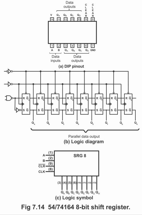
In this register too, data shifts in a serial manner according to the afore-mentioned details and received at the same time on output in parallel fashion, as has been illustrated in the figure. In figure 7.15, specific waveform or timing diagram of this register has been displayed. It is clear from the diagram that serial data existing on input A, shifts in the register and received on output when input B (which is control input or control line) is high. As a result of a high B, NAND gate gets enabled and serial input data, which is being applied on input A, shifts into register in a serial fashion via NAND gate inverter.
Figure 7.15
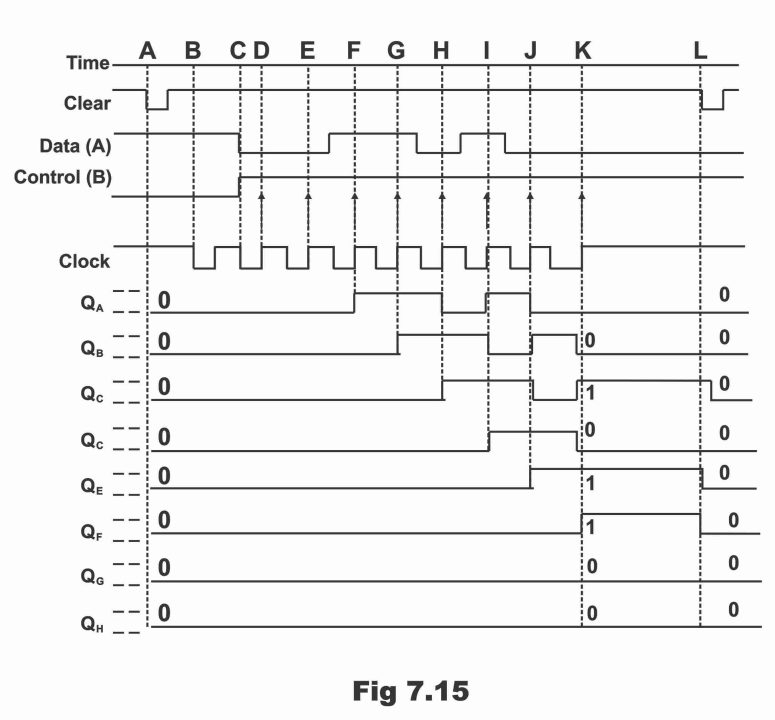
According to this figure, first clear pulse is located on time A and it resets all flip-flops to zero. Clock pulse starts on time B, however due to a low control line, no change occurs as a result of first positive transition (PT) from clock. Control line gets high on time C and first data bit (i.e. 0) shifts into register on time D. similarly, next seven data bits shift into register on time E, F, G, H and I. After time K, clock remains high (as has been demonstrated vide figure). Therefore, number consisting 8-bits (0010 1100) stores in the register and received simultaneously on eight output lines. It should also be inculcated that the right most bit of this number, which is called LSB (Least Significant Bit), first of all shits to the register and received on output QH. Moreover, after positive transition on time K, clock must stop otherwise data may be lost as a result of shifting.
At time L, finally another clear pulse strikes, as a result of which all flip-flops reset on zero and then register gets ready for storing a new number. One method to clear a register is that control line B ought to be turned low and only 8 positive transitions (PTs) are provided by means of clock. Thus, eight zeros will shift inside the register as a result of this process. As a result, register turns cleared.
Parallel in-serial out Shift Register
A shift register, on the inputs of which data can be entered in a parallel form at a time and data can also simultaneously be received in a serial fashion in the shape of bits, is called Parallel in-serial out shift register. It ought to be remembered that data can be stored on this register at a time and this register is concisely termed as PISO. In other words, PISO register is a form of shift register, in which data desired to be shifted, can be introduced concurrently on the input lines in a parallel fashion. And this data is received in a serial fashion on output in the shape of a single bit per clock pulse. It has to be remembered that when data is being provided on parallel inputs of the register, every data bit simultaneously enters the corresponding flip -flop attached with parallel lines.
In figure 7.16 (a)logic diagram of a Parallel in-serial out shift register, comprising 4-bits while in figure (b) logic symbol of the register has been portrayed. As can be seen via figure, this register comprises four data input lines D0, D1, D2, D4 and a SHIFT/LOAD input line, which loads all four data bits on to register in a parallel form. When this SHIFT/LOAD input line is low, all gates from G1 to G3 are enabled (i.e. active or operate). As a result, every data bit is received on D input of its respective flip-flop. In such a situation, when a clock pulse is applied, flip-flops with D = 1, tend to set, whereas flip-flops with D = 0, are reset. Resultantly, all bits inside the register are stored simultaneously.
When SHIFT/LOAD input line is high, all gates from G1 through G3 are disabled (i.e. they don operate) whereas gates from G4 through G6 are enabled (i.e. they start to operate). In such a situation, data bits shift rightward from one stage to the next stage or from one flip-flop to the next flip-flop in a serial fashion. Normal shifting operation or parallel data entry into this register becomes possible by means of OR gates. However, this depends on which of the NAND gates operate (or are enabled) in case of low or high SHIFT /LOAD input line.
Figure 7.16-A 4-bit parallel in/ serial out shift register
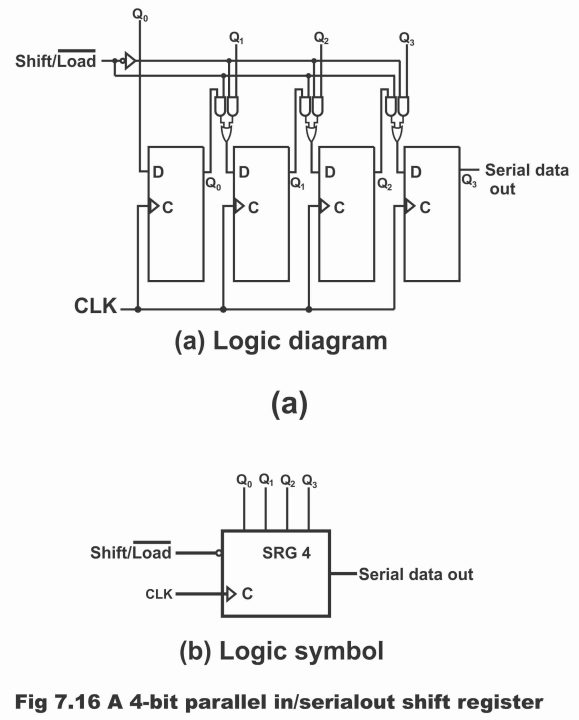
Assume that we want to store number 1010 in this Parallel in-serial out shift register. When SHIFT / LOAD input line is low, all three NAND gates i.e. G1, G2 and G3 are enabled and on striking of first clock pulse, parallel input data (D0 D1 D2 D3 = 1010) present in the register, stores simultaneously on respective flip-flops. As such, following states are established on outputs;
Q0 Q1 Q2 Q3
1 0 1 0
When SHIFT/LOAD input is high, in this situation only gates G4, G5 and G6 operate, as a result stored data shift out from the register in a serial fashion with the exertion of each gate pulse. As the value of Q3 becomes 0 after storage of data within the register, therefore when second clock pulse is applied, bit 1 transfers from Q2 on output Q3 in a serial fashion. After receiving clock pulse 3, bit 0 of Q1 output, shifts on output Q3. Similarly, when clock pulse 4 strikes, last data bit (1) existing on Q0 also shift on Q3. On clock pulse 5, all data inputs stored within register, flows out of the register in a serial fashion and only 0s are left behind. The truth table shown in figure 7.17, also fully elaborates the working operation of this register.
Figure 7.17-truth table for PISO shift register
| Input | Outputs | Remarks About
SHIFT/LOAD Input |
|||
| No. of CLK | Q0 | Q1 | Q2 | Q3 | |
| 1st | 1 | 0 | 1 | 0 | Low |
| 2nd | 0 | 1 | 0 | 1 | High |
| 3rd | 0 | 0 | 1 | 0 | High |
| 4th | 0 | 0 | 0 | 1 | High |
| 5th | 0 | 0 | 0 | 0 | High |
Here, SHIFT / LOAD input Low = Data entered parallelly
SHIFT / LOAD input High = Data shifted out serially.
Parallel in-parallel out Shift Register
Parallel in-parallel out (which also shortly known as PIPO) shift register is such a shift register, wherein input data can be entered or shifted on a register at a time in a parallel fashion (i.e. all bits present on the input are possible to be introduced or applied at a time). And this parallel input data is received simultaneously from output in a parallel fashion. In other words, a register wherein all bits shift at a time and also received on output simultaneously, is called parallel-in parallel out shift register. Remember that, a clock is required for the purpose of shift in data into the register or shifting out data from the register (i.e. transmission of data). Moreover, this register is used just for data storage and it is not possible to shift stored data in the register either leftward or rightward. Therefore, this register is also occasionally known as a data register or data latch.
In figure 7.18 (a), logic diagram of a 4-bit Parallel in-parallel out shift registers and in figure (b) logic symbol of this register has been shown. According to figure (a), this register consists of four D type flip-flops. The operational mechanism of this register is as such that when data comprising 4-bits existing on the register’s inputs, is applied in a parallel form, data is stored completely on the register and also received simultaneously on output as soon as the clock pulse strikes.
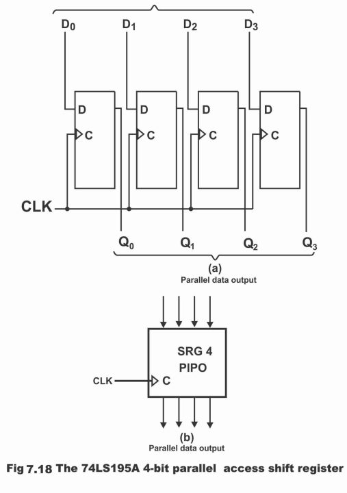
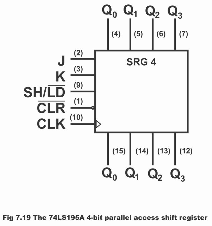
In figure 7.19, pin diagram of a 74LS195A IC number 4-bit parallel access shift register has been shown. This shift register can also be used for Serial in- serial out, (because it also comprises serial input) and Serial in- parallel out operations apart from Parallel in-parallel out.
When its SHIFT/HOLD input (i.e. SH/LD) is low, it operates as a parallel in parallel out shift register. In such a situation, data on its parallel inputs, shifts into the register on clocks’ positive transition (PT) at a time and received on output in a parallel fashion simultaneously. However, when SH/LD is high, stored data on the register shifts rightward (from Q0 to Q3) with clock’s positive transitions. Here, inputs J and K, are serial data inputs, which are received on the first stage (i.e. Q0) of the register in a serial fashion. In this case, output Q3 is used in order to receive output data in a serial form. In this figure, active low clear input is asynchronous (i.e. this input has got nothing to do with clock pulses and register can be cleared any time through its assistance).
Figure 7.19-the 74LS195A 4-bit parallel access shift register
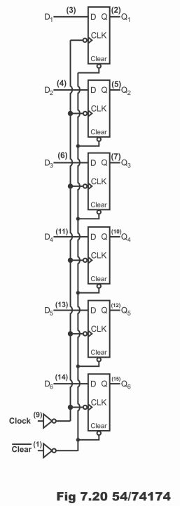
In figure 7.20, 54/74174 IC numbered Parallel in-parallel out register has been illustrated. This register consists of a Clear and a clock apart from 6 D type flip-flops mounted in parallel. Every flip-flop is negative edge triggered. When clock pulse strikes, all six data bits (i.e. D1 through D6) enter or shift into register at a time in a parallel fashion. Moreover, this stored data from Q1 through Q6 is also received on all outputs in a parallel fashion. This type of register is used just to store data and it is not possible to shift data stored data within it right or leftward. by means of providing a low level on clear input, all flip-flops reset immediately and turn out to be low. This clear input is asynchronous (i.e. it can be operated any time irrespective of the clock position)
Figure 7.20-54/74174
Previous Topic: Shift Register: Shift Right and Shift Left Registers with circuit diagram
Next Topic: Counters in Digital Electronics: Synchronous, Asynchronous and Ripple Counter
For electronics and programming-related projects visit my YouTube channel.
Discover more from Electronic Clinic
Subscribe to get the latest posts sent to your email.
