Amplifiers in Electronics, Amplifier types, simulations, and circuits
Last Updated on February 5, 2022 by Engr. Shahzada Fahad
Table of Contents
AMPLIFIERS & FREQUENCY RESPONSES
In this article you will learn about what are Amplifiers and their types, how it works and their Frequency Reponses and Simulation. We will go through Voltage amplifiers, Current amplifiers, and Power amplifiers. You will also know about the classification of signal amplifiers. This is a complete guide about the amplifiers; I have tried my level best to explain the maximum things that I believe you should know.
Amplifier in Electronics:-
An amplifier is an electronic device that increases the voltage, current, or power of a signal. Amplifiers are used in wireless communications and broadcasting, and in audio equipment of all kinds. They can be categorized as either weak-signal amplifiers or power amplifiers.
An amplifier is used to increase the amplitude of a signal waveform, without changing other parameters of the waveform such as frequency or wave shape. They are one of the most commonly used circuits in electronics and perform a variety of functions in a great many electronic systems.
The general symbol for an amplifier is shown in Fig 1.0.1. The symbol gives no detail of the type of amplifier described, but the direction of signal flow can be assumed (as flowing from left to right of the diagram). Amplifiers of different types are also often described in system or block diagrams by name.

WHAT DOES AN AMPLIFIER DO?
The signal that’s amplified is used to power the system to which the amplifier is connected while minimizing distortion (or “noise”). An amplifier typically contains a transistor, which, as explained in a previous article, is based on a semiconductor material with the ability to conduct variable amounts of electric current. The basic steps are as follows:
- The amplifier draws charge from a power supply
- Current is conveyed across the transistor to an output circuit
- The output circuit converts the increased output signal into an equal voltage
- The amplified voltage powers the system
Two further components usually found in an amplifier circuit are diodes and rectifiers. A diode is a two-terminal semiconductor device whose purpose is to conduct current in one direction only and prevent it from flowing back. Meanwhile, a rectifier is a circuit that converts alternating current (AC) into direct current (DC).
An amplifier for every situation
While there are many different types of amplifier, the most common are:
- Transistors: this category can be further broken down into point-contact, bipolar junction (BJT) and metal-oxide-semiconductor field-effect (MOSFET) transistors
- Operational amplifiers: an integrated circuit that amplifies voltage with a high level of efficiency
- Vacuum tubes: mostly replaced by integrated circuits, but still used in UHF systems, high-power radio and radar applications due to its strong output
- Instrument amplifiers: for use with musical instruments
- Distributed amplifiers: found in oscilloscopes due to their ability to split an input current and amplify the separate segments
CLASSIFICATION OF SIGNAL AMPLIFIER
| Type of Signal | Type of Configuration |
Classification | Frequency of Operation |
| Small Signal | Common Emitter | Class A Amplifier | Direct Current (DC) |
| Large Signal | Common Base | Class B Amplifier | Audio Frequencies (AF) |
| Common Collector | Class AB Amplifier | Radio Frequencies (RF) | |
| Class C Amplifier | VHF, UHF and SHF Frequencies |
Amplifiers can be thought of as a simple box or block containing the amplifying device, such as a Bipolar Transistor, Field Effect Transistor or Operational Amplifier, which has two input terminals and two output terminals (ground being common) with the output signal being much greater than that of the input signal as it has been “Amplified”.
THE OUTPUT PROPERTIES OF AMPLIFIERS
Amplifiers are used to increase the amplitude of a voltage or current, or to increase the amount of power available usually from an AC signal. Whatever the task, there are three categories of amplifier that relate to the properties of their output;
- Voltage amplifiers.
- Current amplifiers.
- Power amplifiers.
The purpose of a voltage amplifier is to make the amplitude of the output voltage waveform greater than that of the input voltage waveform (although the amplitude of the output current may be greater or smaller than that of the input current, this change is less important for the amplifier´s designed purpose).
The purpose of a current amplifier is to make the amplitude of the output current waveform greater than that of the input current waveform (although the amplitude of the output voltage may be greater or smaller than that of the input voltage, this change is less important for the amplifier´s designed purpose).
In a power amplifier, the product of voltage and current (i.e. power = voltage x current) at the output is greater than the product of voltage x current at the input. Note that either voltage or current may be less at the output than at the input. It is the product of the two that is significantly increased.
TO SIMULATE THE COMMON EMITTER AMPLIFIER AND OBTAIN THE FREQUENCY RESPONSE
OBJECTIVES:-
- To simulate the common emitter amplifier and obtain the frequency.
- Observe the results.
- Verify the Circuit with Calculations.
MATERIAL REQUIRED:-
- Multisim Software (Updated Version )
- Digital power Source (Vcc)
- Transistor (BC547A )
- Function generator
- Oscilloscope
- 4 Resistors
- 3 Capacitors
- Connecting Wires
- Ground
- MS Word ( For writing down multiple observations)
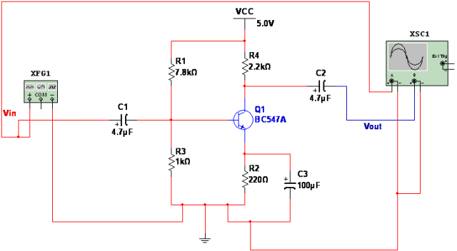
COMMON EMITTER AMPLIFIER (CE)
The Amplifier is an electronic circuit that is used to increase the strength of a weak input signal in terms of voltage, current, or power. The process of increasing the strength of a weak signal is known as Amplification.
The common emitter circuit configuration provides voltage gain combined with a moderate current gain, as well as a medium input and a medium output impedance. As such the common emitter configuration is a good all round circuit for use in many applications.
The Common Emitter Amplifier circuit has a resistor in its Collector circuit. The current flowing through this resistor produces the voltage output of the amplifier. The value of this resistor is chosen so that at the amplifiers quiescent operating point, Q-point this output voltage lies half way along the transistors load line.
The Base of the transistor used in a common emitter amplifier is biased using two resistors as a potential divider network. This type of biasing arrangement is commonly used in the design of bipolar transistor amplifier circuits and greatly reduces the effects of varying Beta, ( β ) by holding the Base bias at a constant steady voltage. This type of biasing produces the greatest stability.
A resistor can be included in the emitter leg in which case the voltage gain becomes -RL/RE. If there is no external Emitter resistance, the voltage gain of the amplifier is not infinite as there is a very small internal resistance, Re in the Emitter leg. The value of this internal resistance is equal to 25mV/IE
GAIN:-
Current gain in the common emitter circuit is obtained from the base and the collector circuit currents. Because a very small change in base current produces a large change in collector current, the current gain (β) is always greater than unity for the common-emitter circuit, a typical value is about 50.
PROCEDURE:-
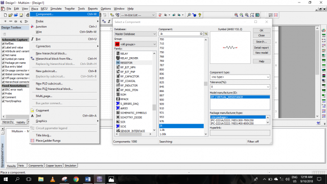
- Start by Opening the Multisim Software

- A Clear circuit window appears.

- Click “place” in main menu < Components < Select resistor < Set Value < Press Ok.
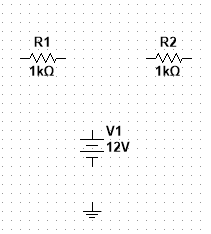
-
- Place the Resistor on the Circuit window and left Click to fix it.
- Do same for other components i.e. Resistor, Transistor Source, Capacitor Ground etc.
- Place them any Where and left click to fix them on board.
- Now After Placing the required components bring the circuit close to the pins of the components and wire them up.
- Left-click on the pin of the first component, then left-click on the pin of the component to wire up.
- Multisim will automatically place the wire between the two components that were selected
- Select the Ammeter and voltmeter from the menu and fix them on circuit for finding current and voltage across resistor.
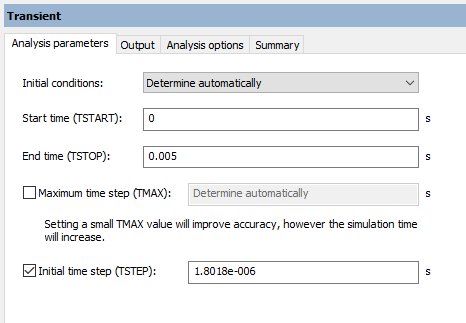
- The circuit is ready now analyses it set the timings. Save it and then run simulation.
COMMON EMITTER AMPLIFIER CIRCUIT DIAGRAM:-
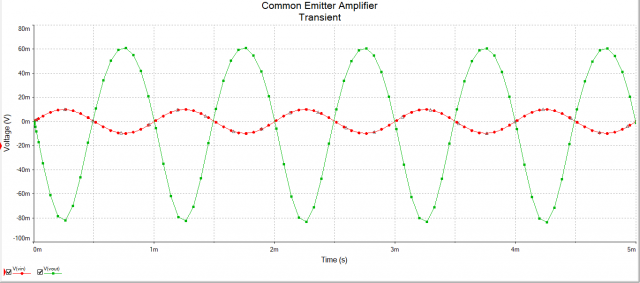
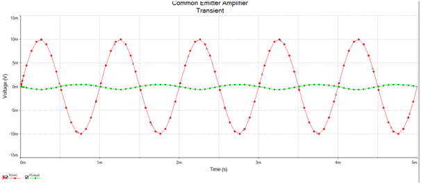
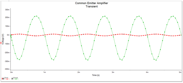
SIMULATION GRAPH:-
download Simulation: Common Emitter Amplifier
CALCULATIONS:-
| Source (mv) | Rb Ω | Rc Ω | Output (mv) |
| 5 | 0.886k | 2.2k | 60 |
| 5 | 0.915k | 2.2k | 10 |
| 5 | 0.886 | 8.2k | 200 |
PARAMETERS:-
OBSERVATIONS:-
We observed and learned various things like
By increasing the collector resistance the dc gain also increases because of direct relationship and inverse is the relation for base resistor which lower the value whenever we apply voltage divider and find the equivalent resistance and compare over result over both Rb and RC we get the analysis of Common emitter amplifier.
Every Circuit is Incomplete until it is not grounded
TO SIMULATE THE COMMON SOURCE AMPLIFIER AND OBTAIN THE FREQUENCY RESPONSE
OBJECTIVES:-
- To simulate the common source amplifier.
- Observe the results.
- Verify the Circuit with Calculations.
MATERIAL REQUIRED:-
- Multisim Software (Updated Version )
- Digital power Source (Vcc)
- Oscilloscope
- Function generator
- FET Transistor (GaAsFET-N )
- 6 Resistors
- 3 Capacitors
- Connecting Wires
- Ground
- MS Word ( For writing down multiple observations)
Summary:-
JFET:-
JFET is Junction gate field-effect transistor. Normal transistor is a current controlled device which needs current for biasing, whereas JFET is a voltage controlled device. Same like MOSFETs, as we have seen in our previous tutorial, JFET has three terminals Gate, Drain, and Source.
JFET is an essential component for precision level voltage operated controls in analog electronics. We can use JFET as voltage controlled resistors or as a switch, or even make an amplifier using the JFET. It is also an energy efficient version to replace the BJTs. JFET provides low power consumption and fairly low power dissipations, thus improving the overall efficiency of the circuit. It also provides very high input impedance which is a major advantage over a BJTs.
COMMON SOURCE AMPLIFIER (CE)
In electronics, a common-source amplifier is one of three basic single-stage field-effect transistor (FET) amplifier topologies, typically used as a voltage or Tran’s conductance amplifier. … As a Tran’s conductance amplifier, the input voltage is seen as modulating the current going to the load.
In electronics, a common-drain amplifier, also known as a source follower, is one of three basic single-stage field effect transistor (FET) amplifier topologies, typically used as a voltage buffer. … That resistance reduction makes the combination a more ideal voltage source.
Similarly, the common-drain amplifier is called a source-follower because the voltage at the source is approximately the same amplitude as the input (gate) voltage and is in phase with it. A common-drain amplifier is also called a source-follower. Self-biasing is used in this particular circuit.
The most common type of FET amplifier is the MOSFET amplifier, which uses metal–oxide–semiconductor FETs (MOSFETs). The main advantage of a FET used for amplification is that it has very high input impedance and low output impedance.
Hence, field effect transistors have no “current gain”. A voltage controlled voltage source is a called an Operational Amplifier (or op-amp). … JFET amplifiers tend to have fairly low voltage gain and many have voltage gains less than unity.
PROCEDURE:-
- Start by Opening the Multisim Software
- Click “place” in main menu < Components < Select resistor < Set Value < Press Ok.
- Place the Resistor on the Circuit window and left Click to fix it.
- Do same for other components i.e. Resistor, Transistor Source, Capacitor Ground etc.
- Place them any Where and left click to fix them on board.
- Now After Placing the required components bring the circuit close to the pins of the components and wire them up.
- Left-click on the pin of the first component, then left-click on the pin of the component to wire up.
- Multisim will automatically place the wire between the two components that were selected
- Select the Ammeter and voltmeter from the menu and fix them on circuit for finding current and voltage across resistor.
- The circuit is ready now analyses it set the timings. Save it and then run simulation.
- Vary the value of elements for more reading
Common Source Amplifier Circuit Diagram:-

CALCULATIONS:-
| Vin | Rb | Rc | Vout |
| 20mv
|
0.86 MΩ | 5.1k | 37mv |
| 40mv | 1.74MΩ | 10.3k | 80mv |
| 80mv
|
1.56MΩ | 13.2k | 175mv |
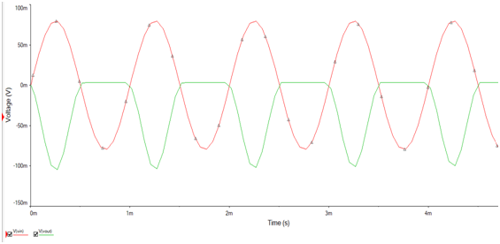
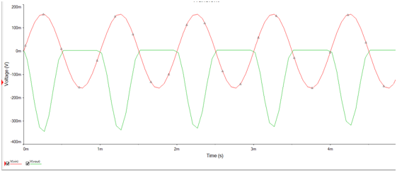
GRAPH:-
(For 20mv, 40mv, 80mv respectively)
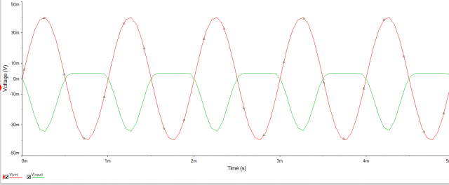
SIMULATION
download Simulation: Common source amplifier
PARAMETERS:
OBSERVATIONS:-
I have observed that the common source FET amplifier circuit is one of the most commonly used providing current and voltage gain along with a satisfactory input and output impedance.
The common source circuit provides a medium input and output impedance levels. Both current and voltage gain can be described as medium, but the output is the inverse of the input, i.e. 180° phase change. This provides a good overall performance and as such it is often thought of as the most widely used configuration.
TO SIMULATE THE CURRENT SERIES FEEDBACK AMPLIFIER AND OBTAIN THE GAIN
OBJECTIVES:-
- To simulate the Current series feedback amplifier.
- Obtain the Gain
- Observe the results.
- Verify the Circuit with Calculations.
MATERIAL REQUIRED:-
- Multisim Software (Updated Version )
- Digital power Source (Vcc)
- Function generator
- Transistor (BC107BP)
- 5 Resistors
- 3 Capacitors
- Connecting Wires
- Ground
- MS Word ( For writing down multiple observations)
SUMMARY:-
An amplifier circuit simply increases the signal strength. But while amplifying, it just increases the strength of its input signal whether it contains information or some noise along with information. This noise or some disturbance is introduced in the amplifiers because of their strong tendency to introduce hum due to sudden temperature changes or stray electric and magnetic fields. Therefore, every high gain amplifier tends to give noise along with signal in its output, which is very undesirable.
The noise level in the amplifier circuits can be considerably reduced by using negative feedback done by injecting a fraction of output in phase opposition to the input signal.
PRINCIPLE OF FEEDBACK AMPLIFIER
A feedback amplifier generally consists of two parts. They are the amplifier and the feedback circuit. The feedback circuit usually consists of resistors.
CURRENT-SERIES FEEDBACK
In the current series feedback circuit, a fraction of the output voltage is applied in series with the input voltage through the feedback circuit. This is also known as series-driven series-fed feedback i.e., a series-series circuit.
As the feedback circuit is connected in series with the output and the input as well, both the output impedance and the input impedance are increased.
PROCEDURE:-
- Start by Opening the Multisim Software
- Click “place” in main menu < Components < Select resistor < Set Value < Press Ok.
- Place the Resistor on the Circuit window and left Click to fix it.
- Do same for other components i.e. Resistor, Transistor Source, Capacitor Ground etc.
- Place them any Where and left click to fix them on board.
- Now After Placing the required components bring the circuit close to the pins of the components and wire them up.
- Left-click on the pin of the first component, then left-click on the pin of the component to wire up.
- Multisim will automatically place the wire between the two components that were selected
- The circuit is ready now analyses it set the timings. Save it and then run simulation.
- Vary the value of elements for more reading.
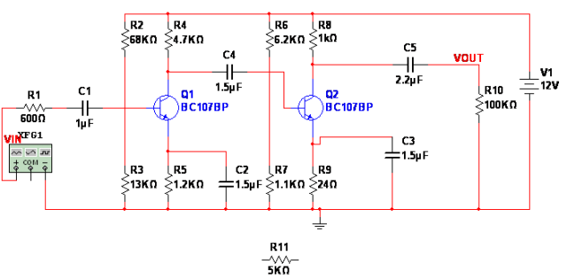
FEEDBACK AMPLIFIER CIRCUIT DIAGRAM:-

CALCULATIONS:-
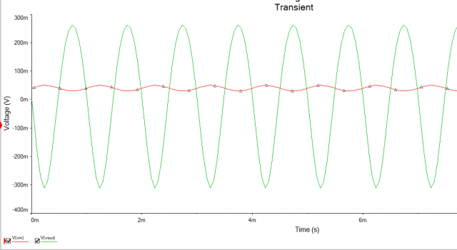
| Input voltage | Output voltage | Voltage gain |
| 5mv | 270mv | 54 |
| 9mv | 370v | 40 |
| 10mv | 410mv | 41 |
GRAPH:-
FOR (5mv, 9mv, 10mv respectively)

download Simulation: CURRENT SERIES FEEDBACK AMPLIFIER
SIMULATION PARAMETERS

OBSERVATIONS:-
I have observed that to determine the effect of feedback voltage on the input of base emitter voltage we need to apply kvl this is called series mixing and as the two nodes are in not in same positions this is current series feedback topology. We observed that the feedback is from output to input which improves the response of the circuit.
TO SIMULATE THE CURRENT SHUNT FEEDBACK AMPLIFIER AND OBTAIN THE FREQUENCY RESPONSE.
OBJECTIVES:-
- To simulate the Current shunt feedback amplifier.
- Obtain the Gain
- Observe the results.
- Verify the Circuit with Calculations.
MATERIAL REQUIRED:-
- Multisim Software (Updated Version )
- Digital power Source (Vcc)
- Function generator
- 2 Transistor (BC107BP)
- 11 Resistors
- 5 Capacitors
- Connecting Wires
- Ground
- MS Word ( For writing down multiple observations)
SUMMARY:-
Current shunt feedback amplifier is the type of negative feedback amplifier in which the part of the output current is applied in parallel with the input current. In this case the output current is directly proportional to the input current therefore the amplifier is the true current amplifier.
In current shunt feedback amplifier the gain decreases, input resistance decreases and the output resistance increases.
he load current is sampled by placing a small value resistor in series with the load at the collector . The voltage across this sampling resistor is made to appear in shunt (parallel) to the input.
This circuit has the property of increasing the o/p impedance and decreasing the input impedance. The second property is useful in connecting the transducers to the amplifiers to impedance match for maximum voltage transfer.
PROCEDURE:-
- Start by Opening the Multisim Software
- Click “place” in main menu < Components < Select resistor < Set Value < Press Ok.
- Place the Resistor on the Circuit window and left Click to fix it.
- Do same for other components i.e. Resistor, Transistor Source, Capacitor Ground etc.
- Place them any Where and left click to fix them on board.
- Now After Placing the required components bring the circuit close to the pins of the components and wire them up.
- Left-click on the pin of the first component, then left-click on the pin of the component to wire up.
- Multisim will automatically place the wire between the two components that were selected
- The circuit is ready now analyses it set the timings. Save it and then run simulation.
- Vary the value of elements for more reading.
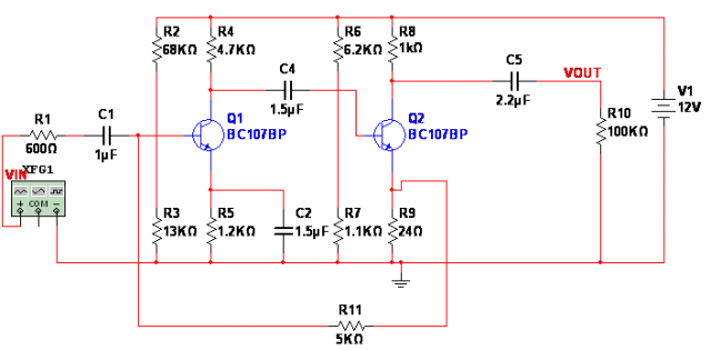
Current Shunt Feedback Amplifier Circuit Diagram:-
CALCULATIONS:-
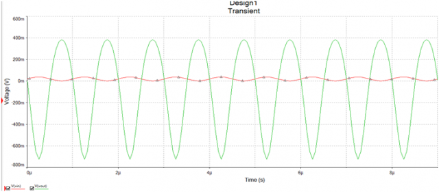
| Input voltage | Output voltage | Voltage gain |
| 5mv | 270mv | 54 |
| 9mv | 370v | 40 |
| 10mv | 410mv | 41 |
GRAPH:
download Simulation: CURRENT SHUNT FEEDBACK AMPLIFIER
SIMULATION PARAMETERS:
OBSERVATIONS:-
I have observed that to determine the effect of feedback voltage on the input of base emitter voltage we need to apply kvl this is called series mixing and as the two nodes are in not in same positions this is current series feedback topology. We observed that the feedback is from output to input which improves the response of the circuit.
Discover more from Electronic Clinic
Subscribe to get the latest posts sent to your email.