CCD Vs CMOS Sensor, Comparison and working explained
Last Updated on September 12, 2021 by Engr. Shahzada Fahad
Table of Contents
CCD and CMOS Sensors:
CCD CMOS:- In this article we learn about the sensor that is used in digital cameras and smart phones. We will learn how this image sensor works and at the end we will compare the image sensor in different aspects. So two types of image sensors which are quite commonly used in imaging are:
- CCD which is charged coupled device
- CMOS which is complementary metal oxide semiconductor
So both types of the sensor consist of millions of photo sites or pixels. So these photo sites convert the incoming light in to the charge or electron. So although these two sensors are quite different but they are common in many aspects so these are the following steps which are being followed in both the sensors. So these sensor first convert the light in to charge so the photo sites or pixels is exposed to light for a certain amount of the time and during this time the charge will get collected in this pixels. So once the charge is collected by the pixel this charge is transferred for farther processing and after the transfer the charge is converted in to voltage and this voltage is being amplified using the amplifiers. So these are the common steps which we see in both sensors but depending upon the sensor the sequence might vary. Now we will discuss each sensor:
CCD (Charged coupled device):
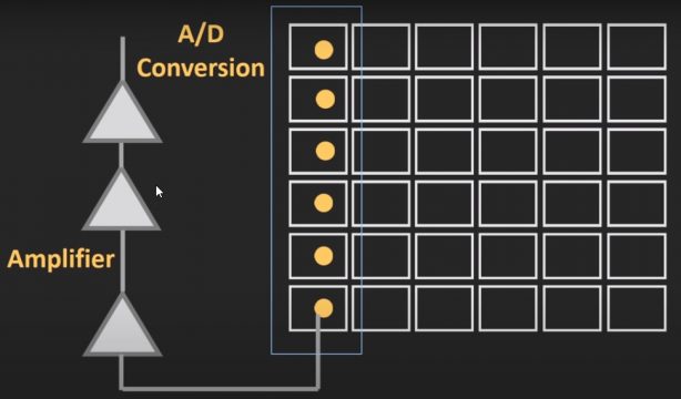
The CCD stands for Charged coupled device. The CCD consists of millions of pixels. So as these pixels are exposed to the incoming light, these pixels will convert the incoming light in to the charge and the charge will accumulated in these pixels. So once the charging is getting collected by these pixels, these charges are being transferred using the horizontal shift register. These charges are being transferred in to the vertical shift register. So in this shift register one by one each charge is converted in to voltage and after the voltage conversion each voltage is being amplified using the amplifier. So once the vertical shift register gets emptied the same procedure is followed for the remaining charge and one by one each charge is getting converted in to voltage and after that it is being amplified. So once the charge of each pixel is converted in to the voltage and amplified the output signal is being converted in to the digital signal using the analogue to digital converter. The same process is repeated for the next frame. So this is the basic principle of the charge coupled device.
CMOS Sensor:
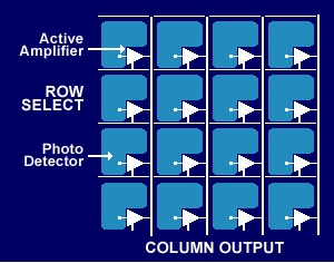
The dominant type of the technology is the CMOS. CMOS stands for complementary metal oxide semiconductor a specific way of making electronic circuit. CMOS sensor the fabrication technology is very to the fabrication technology of the integrated circuit. So because of that many peripheral circuits can be integrated inside the single chip. So in case of the CMOS sensor the charge to voltage conversion as well as the voltage amplification is carried out in the pixel itself. So the processing speed of the CMOS sensor will be much higher than the CCD sensor. So in case of the CMOS sensor the voltage that is generated by each pixel is being read in line by line fashion. So first of all the first row of the pixel is being activated using the pixel select switch. This pixel switch connects this output voltage of the pixel to the column line. By activating the column select switch one by one we can read the data of each pixel and the same procedure is repeated for the remaining lines. So in this case of the CMOS sensor the data is being read in the line by line.
Passive CMOS sensor:
The passive CMOS image sensor is not used much anymore except for may be low cost, low performance application. Imagine that we have an array of photodiodes with each photo diode connected by a switch to a vertical output line. Each vertical output line is connected by a switch to a horizontal output line going to an amplifier by activating pairs of switches. It is possible to connect any photodiode to the output amplifier. In actual fabrication the switches are nothing more than MOS transistor. This design of an image sensor is inexpensive to make it delivers rather poor speed and noise performance.
Active CMOS sensor:
The limitation of the passive CMOS can be overcome by using three transistors per pixel. One of the transistor is used as an amplifier this enables the image sensor to drive a voltage from the each pixel instead of the charge packet that is far more efficient and gives higher speed and better noise performance. Another transistor will serves as reset transistor for the photodiode. The third transistor is the row select transistor identical to what is use in passive CMOS sensor.
Working of the Active CMOS sensor:
In this type of sensor we have:
- Photodiode
- Reset switch
- Amplifier
- Row select
The photodiode is reset when the reset is removed incoming photons creates photo generated charge. The photo generated charge creates a voltage on the output of the amplifier that voltage is read out when the row select transistor is activated select transistor is activated in an actual image sensor. Typically each column has an amplifier with a small capacitor to hold the voltage during the reading out of the row at the end of the first row exposure the row is selected and the voltage from the each photo sensor is transferred to the row read out. As the row is being read out the photodiodes are reset and can begin a new exposure.
After the first row is read out the output from the second row is selected is transferring them to the row read out. The second row is reset and begins a new exposure this process continues until the entire image sensor is read out at which time the first row is ready to be read out again.
The basic CMOS sensor incorporates three transistors along with a photodiode for each pixel transferring a voltage rather than a charge packet gives better performance we may notice though that each row is exposed at a slightly different time. This leads us in to a discussion of a rolling shutter.
Timing and rolling shutter of the CMOS sensor:
The exposure timing may look like for the CMOS sensor previously described each row is exposed at a time slightly later than the previous row for this reason it is called a rolling shutter.
Now we will discuss that what will happen when imaging a moving object such as roller bearing we want a still image but as each scan line is exposed to light at slightly different time with a top line first and the bottom line last the rolling shutter causes the image of a moving object to skew a distortion to fix the distortion caused when imaging with a rolling shutter requires the addition of two more transistors and a capacitor as shown in the schematic.
The way this works is that all photo sensors on the image sensor are reset at the same time. There is a period of exposure and again all photo sensors are exposed at the same time then the charge from the every photo sensor is transferred on its capacitor simultaneously. After the transfer the photo sensor is reset to be ready for the next exposure even while the image data is read out. A row is selected and the pixel amplitude is read out sequentially. After the readout is completer and before the next exposure can be transferred. The capacitors are reset to be ready to accept a new charge from the photo sensor.
Now according to the diagram of the CMOS global shutter image sensor in action we reset one resets the photo sensor, reset two resets the storage capacitor. When reset one is removed exposure begins, reset two must be removed before the transfer of charge from the photo sensor to the storage capacitor. The charge from all pixels is transferred from the photo sensor to the corresponding storage capacitor in parallel. After the transfer is complete the photo sensor can be reset in preparation for the next exposure. The first row is selected and the voltage from each of its pixels to a storage capacitor on the row read out. The columns are selected sequentially causing the pixel values from the first row to be read out in the sequence that process is repeated for the second and subsequent row. After the law row of pixel is transferred to the horizontal read out. The storage capacitor for all pixels can be reset.
Comparison of the CCD and CMOS sensors:
CCD:
Specialized fabrication techniques are used so expensive technology
System Integration:
CCD very old technology so it is not possible to integrate the peripheral components like timers and ADC in to the main sensor so we will require additional circuitry for it. So the overall size of the CCD will get large.
Power Consumption:
Higher power consumption because of the capacitive architecture and we require different types of power supplies for the different timing clocks and not only that the typical voltages which are being required for this CCD is in the range of 7 V to 10 V.
Processing Speed:
Always have to read out the whole image due to which its processing speed is less. This processing speed can be increased by using the multiple shift registers. But this will required additional amount of the hardware.
Dynamic range of the CCD sensor quite high compared to CMOS sensor.
Image distortion:
In case of the CCD sensor when we exposed the sensor for a long time then we will see the effect that is known as blooming. So now day by using the anti-blooming technique we can reduce this blooming.
Resolution is limited by sensor elements size
CMOS:
System Integration:
In case of the CMOS sensor it is possible to have the camera on the chip or system on the chip and because of that CMOS is quite compact.
Power Consumption:
Low power consumption because it require single power supply and the typical voltage that is required for the CMOS sensor is relatively in the range of 3.3 V to 5 V. So in the application where the power consumption is the main criteria in such scenario the CMOS censor will be preferred over the CCD sensor.
Processing Speed:
Readout for selective area of an image is possible due to which its speed is maximum as compared to the CCD sensor and further we can increase its speed by using the multiple column select lines
Noise and Sensitivity:
CMOS has stronger noise due to higher dark currents because the charge to voltage converter circuit as well as amplification circuit is integrated in to the same pixel. So overall fill factor of the CMOS sensor will less compared to the CCD sensor and due to which the sensitivity of the CMOS sensor will be less compared to the CCD sensor. In case of the CMOS sensor the amplifiers which are being used in each pixel is not identical. So because of that we will see the non-uniform amplification and this will act as additional noise. But now the technology of this CMOS sensor has evolved so much that the noise and sensitivity of this CMOS sensor is at par with the CCD sensor.
Image distortion:
In case of the CMOS sensor the most common type of the distortion is to be known is rolling shutter as in the case of the CMOS sensor the pixels is read line by line fashion so because of that whenever any fast moving object is captured by this CMOS sensor then this rolling shutter effect is quite noticeable. While in the case of the CCD all the pixels are exposed at the same time. So if we want to remove the rolling shutter effect in the CMOS sensor than all the pixels should be exposed at the same time which is known as the global shutter. So now a days the CMOS sensor also coming with the global sensor.
- Cheaper technology
- Smaller size
- Amplifier and additional circuitry can be fabricated inside each pixel.
- Higher resolution possible
Discover more from Electronic Clinic
Subscribe to get the latest posts sent to your email.
