Field Effect Transistor FET, JUGFET and IGFET Explained
Last Updated on October 6, 2020 by Engr. Shahzada Fahad
Table of Contents
Field effect Transistor (FET):
The field effect transistor is three terminals and unipolar because it depends upon on either holes or electrons which use the electric field to control the flow of current through device. And it is very useful in many applications. In fact today most of the integrated circuits including the computers are designed using the FETs. The drain, gate and source are the three terminals of the FET.
So in FET the current used to flow between the drain and the source terminal also it is more temperature stable than BJTs and are smaller than BJTs therefore suitable for use in integrated circuits. And this can be controlled by applying the voltage between the gate and the source terminal. So the applied voltage generates the electric field within the device and by controlling this electric field or in a way by controlling the voltage we can control the flow of the current through the device. So basically in this field effect transistor by controlling the electric field we can control the flow of the current. And that is why it is known as field effect transistor. Field effect transistor is voltage control device.
FET is unipolar device which consists of either free electron or holes. Now in terms of application FETs are used in almost all the applications where the BJTs are used. FETs does not contain minority carrier therefore they are suitable for switching application because there is no charge store problem. The FETs are less noisy. For example they are used as amplifier or oscillator in many application and apart from that also used as analogue switch in many application but the biggest difference between the field effect transistor and the BJT is that the input impedance of the field effect transistor is very high and due to that they are used as a buffer amplifier in many applications.
The power consumption of the FETs are less than BJTs and that’s why they are preferred in many high power applications as well as in the computing applications particularly where the required power consumption should be minimum. FETs has smaller gain and bandwidth. FETs provides thermal stability and generates less noise and high frequency. So these are few differences between FETs and BJTs.
Unlike the bipolar junction transistors which are all basically similar in spite of a variety of constructional forms the FET is more a collective term for a family of transistor devise of which there are two principal groups:
- The junction type FET (JUGFET)
- Insulated type FET (IGFET)
The JUGFET can be in two forms, p-channel and n-channel, depending on the type of semiconductor forming the basis of the transistor. The IGFET has two distinct modes of operation, one known as the depletion mode and the other as thee enhancement mode, again and again each mode subdivides into p-channel and n-channel.
Like the bipolar junction transistor all FETs are three electrode devices the electrodes are the source, the gate and the drain which can be taken as corresponding to the emitter, base and collector respectively.
JUGFET:
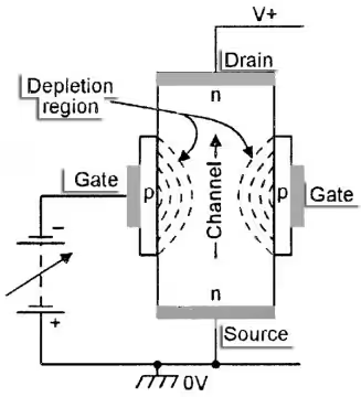
The most common variety of JUGFET is the n-channel type. This consists of a piece of n-type silicon effectively within a tube of p-type silicon, the interface between the two materials being the same intimate junction as in the bipolar transistor junctions. Non rectifying contacts are connected to each end of the n-type piece and to the p-type tube. The two end contacts are termed the source S and the drain D, while that to the tube or shroud is the gate G.
The principal of the action of a JUGFET can be first explained by considering the operation of the source and drain while the gate left disconnected. Since we are considering an n-channel JUGFET consider dc supply connected with the drain positive with respect to the source. The application of the drain source voltage causes conventional current to flow from the drain to the source the current consists of electrons which are the majority carriers in the n-channel moving from the source to the drain. Being semiconductor material the voltage / current relationship is almost linear and the n-channel more or less behaves as a resistor.
To bring the gate into action first connect it to the source. The drain source current is still flowing and therefore the n-channel voltage becomes greater as electron flow from the source towards the drain. It follows that electrons nearer the drain also experience a higher voltage with respect to the gate, hence the voltage across the p-n junction is greater at the right hand end than at the left. Also the p-n junction is reverse biased and this bias is greater nearer the drain than nearer the source. The causes a depletion layer which becomes greater at the bias increases i.e the depletion layer is greater nearer to the drain.
The depletion layer which act as an insulator it reduces the effective cross section of the n-channel and therefore restricts the flow of electrons. For this reason the FET is said to be operating in the depletion.
If the drain-source voltage is increased the current might increase; but the increase in voltage also increases the depletion layer which restricts the increase. Eventually a point is reached at which the depletion layer completely absorbs the n-channel and the drain source current reaches a limiting value called the saturation current . The saturation point is termed the pinch off point. If the drain source voltage is disconnected and a bias voltage applied to the gate. The depletion layer is evenly set up in the n-channel. This effectively reduces the cross section and means that when a drain source voltage reapplied the pinch off point will be experienced at a lower voltage, and the currents including the saturation current will be less.
The combined effect of applying both drain source voltage and bias voltage. Here the drain current depend on both voltages and the more negative the bias gate voltage the smaller is the saturation current. The gate voltage could stop the flow of drain current if increased sufficiently but ,more importantly the gate voltage has a more significant effect on the drain current than the drain voltage.
The resulting output characteristics of an n-channel JUGFET. Operation occurs beyond pinch off so that the control in by the gate voltage. The characteristics compare in form with those for the junction transistor and the amplifier action can be obtained in the manner.
The symbol used in circuit diagrams for an n-channel JUGFET along with that of the p-channel variety. The operation of the p-channel JUGFET is the converse of the n-channel action with all polarities and current flow direction reversed.
The gate source junction present very high values of resistance mega ohms since they consist of reverse biased junctions. It follows that the gate currents are very small but due to the increase in minority charge carriers with temperature, these currents do vary with temperature.
IGFET (Insulated gate field effect transistor):
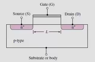
As the name indicates the IGFET has its gate insulated from the channel. A simplified form of construction in which the main bulk of the material is low conductivity silicon this is termed the substrate.
For an n-channel IGFET the substrate is p-type silicon into which is introduced a thin n-channel terminated in the drain and source electrodes. The gate is separated from the channel by a layer of silicon dioxide which is an insulator ensuring that the gate is isolated from both source and drain. The silicon dioxide can be thought of as the dielectric in a capacitor consisting of two plates one being the gate and the other the channel.
In the IGFET the flow of electrons from drain to source is again the same as in the JUGFET and the pinch-off effect can also be achieved by connecting the gate to the source. However the variation of the gate source voltage produces a distinctly different effect.
If the gate is made positive with respect to the source and hence to the channel the source drain current is increased. Because of this increase the FET is said to be enhanced. Conversely if the gate us made negative with respect to the source and hence to the channel the source drain current is decreased and the FET is said to be depleted or in the depletion mode.
The output characteristics of an n-channel IGFET and the symbol for the IGFET are shown. Again the p-channel IGFET is the converse of the n-channel. Note that a connection to the substrate is available and may be used as the other terminal for the bias arrangement.
The cause of the variation in drain current when bias voltages are applied to the gate lies in the capacitive effect between gate and channel. If the gate is positively charged then the channel is negatively charged and the channel therefore experiences an increase in charge carriers, i.e it is enhanced when the bias is reversed there is depletion in the number of charge carriers available.
The cause of the pinch off effect is less obvious but stems from the p-n junction between the channel and gate as in the JUGFET. Often the substrate is connected to the source which is also convenient for the gate source bias.
There is an important derivative of the IGFET which is the enhancement mode IGFET for which the output characteristics are shown. In it the channel is omitted and conduction can only take place when the gate is positive with respect to the substrate. This induces a conduction channel in the substrate and it follows that operation can only take place in the enhancement mode.
Although there are differences between the IGFET symbols these are not applied in practice because this could confusing. Finally the IGFET is sometime s also termed a MOSTFET due to the metal oxide and silicon form of construction and even MOSFET might be further contracted as MOST. IGFETs can easily be destroyed by the build-up of charge across the dielectric separating the gate and substrate. To avoid this often these are linked at manufacture and the links have to be removed when the IGFETs are installed.
Static Characteristics of a FET:
There are three principal characteristics: the drain resistance, the mutual conductance, and the amplification factor.
The ratio of the change of ∆DDS of the drain source voltage to the change ∆ID of the drain current for a given gate source voltage is termed the drain resistance rd.
rd = (∆VD)/(∆ID )
The value r_d is large in most FETs say in the order of 10KΩ-500KΩ. The ratio of the change ∆I_S of the drain current to the change ∆VGS of the gate source voltage is termed the mutual characteristics gm .
gm =(∆ID )/(∆IVDS )
Where g_m is usually measured in milli amperes per volt.
The product of drain resistance and mutual conductance gives the amplification factor µ.
µ=r<sub>d</sub> g<sub>m</sub>
like the junction transistor the FET can be represented by a circuit which is equivalent to its response to small signal causing it to operate over the linear part of its characteristics. The FET equivalent circuit is similar to that for the junction transistor except that the input resistance is so high that it can be considered infinite i.e equivalent to an open circuit.
The parameters are termed Y parameters Y_fs is the forward transconductance (the s indicates that it is for the common source mode) and is the ratio of I<sub>D</sub> to V<sub>GS</sub>. It follows that expressed in amperes per volt or sometimes in siemens. Y<sub>os</sub> is the output conductance (in the common source mode) and is also measured in amperes per volt.
Consider the transistor in the amplifier arrangement. The equivalent circuit is shown and again capacitors are taken to have negligible effect.
I=ID+VDYos
I=ID+ID I1 Yos
ID=I/(1+RL Yos )
ID=(VGS Yfs)/(1+RL Yos)
Vo=ID RL
Vo=(VGS Yfs RL)/(1+RL Yos)
Av=(Yfs RL)/(1+RL Yos)
The FET as a switch:
We have observed that the bipolar transistor can operate as a switch. In particular it has current flowing from collector to emitter (assuming an npn type) so long as the base emitter junction is forward biased. Reverse the bias and effectively no current flow this gives rise to the ON/OFF switching action.
The operation is imperfect because there is a significant input current when the base emitter junction is forward biased. This gives rise to a collector emitter voltage known as the offset voltage.
By comparison the FET has distinct advantages. In particular the insulated gate ensures that no current is taken by the gate electrode whether the device is effectively ON or OFF. Also in the OFF condition effectively no current flows between the drain and the source. This means that the transistor is acting as an open circuit which is what we would expect of a switch. Finally when operating in the ON condition the resistance introduced by the FET is negligible.
There are differences between the operation of JUGFET and IGFET switches. In JUGFET the gate voltage must be sufficiently negative to ensure that no drain current flows in the OFF condition. Any suitable voltage between this value zero results in the device being switched ON. The transfer characteristics of a JUGFET are compared with those of a bipolar transistor. With an IGFET operating in the depletion mode the gate voltage must be sufficiently negative to ensure that the switch is OFF. Operation in the enhancement mode avoids the need for a negative signal to ensure the OFF operation since this is its normal condition. Again a positive gate voltage causes the ON operation to occur. The transfer characteristics for both modes of operation. FETs are more preferred than BJTs.
Biasing The FET biasing in which we will turn on the FET which provides fixed level of current to flowing through a device and provide fixed voltage drop across the device the biasing in FETs are like transistor biasing. When we bias the FET it operates in the proper region. It is necessary to bias the gate source junction in reverse bias for its proper operation because the gate terminal of the FET is constructed not to handle the significant amount of signal. If the gate source junction becomes forward bias then it allow the current to flow through the gate terminal and that may damage the FET. It can be fixed bias, self-bias, and the potential- Divider biasing.
(1) Fixed Bias
We can connect the FET in Fixed bias which is the simplest biasing technique by supplying voltage to the FET with the battery voltage. The terminal gate must connect with the negative supply of the battery and no current flow is evident through the resistor.
VDS=VD-ID RD
VS=0V
VS=VDS
VDS=VGS
VGS=-VGG
(2) Self Bias
As the name suggests if the external supply is not provided for the circuitry. This type of bias is known as self-bias we can understand the self-biasing by considering the circuit. In which only supply VDD are used which is applied to the drain terminal. The gate terminal voltage is zero therefore it is connected with ground through resistor. Any changes in the transconductance values that reflect the distortion of the operating point when the voltage vdd is applied to the drain the drain current start in the FET. The drain current will cause the voltage drop in the source resistor. The source resistor is called the feedback resistor because it controls the amount of the drain current in the FET. When the drain current starts to flow in the Rs it causes the voltage drop in the source resistor. This voltage drop has the effect creating reverse biasing effect gate to source junction. As the reverse biasing is increased the depletion region also increases. Increase in the depletion region will reduce the width of the channel present in FET. So the width is get reduce the therefore the flow of the drain current is also get reduced. Because the width of the channel control the flow of the drain current. So as the drain current get reduces the voltage drop across Rs will also get reduces.
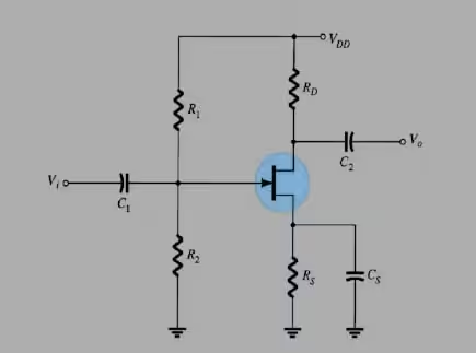
(3) Potential Divider Bias
The circuit is provided with the supply at the input but the two resistors are connected in such a way that the voltage at the input is divided with the help of resistors. Hence this circuitry is referred to as potential divider.
These biasing techniques are chosen based on the necessity and the increment of the conductance values.
VG=R2/(R1+R2 )×VDD
VGS=VG-ID RS
IR1=IR2=VDD/(R1+R2 )
VDS=VDD-ID (RD+RS)
VD=VDD-ID RD
VD=ID RS
Characteristics
We can determine the characteristics of the FET on its various operating regions. The regions are ohmic, saturation, cut-off and the breakdown region.
(1) Ohmic Region
The region at which the transconductance shows the linear response and the current at the terminal gate is opposed by the resistance is known as ohmic region.
(2) Saturation Region
At this region, the device is at fully ON mode. During this condition the maximum amount of current flow through the transistor at a steady state.
(3) Cut- off Region
The FET is said to be in cut off region when no current is flowing in the FET. Hence it is referred to as the device in the OFF condition.
(4) Breakdown Region
The FET will operate in the breakdown region when the applied voltage exceeds the condition of the maximum value of the voltage then the FET will be enters into the breakdown condition indicating that the FET will resists the flow of current.
Discover more from Electronic Clinic
Subscribe to get the latest posts sent to your email.
