Generate PCB Gerber files using Eagle and Online Gerber Viewer by PCBWay
Table of Contents
Description:
Generate PCB Gerber files using Eagle and Online Gerber Viewer by PCBWay– In this tutorial you will learn how to generate PCB Gerber files using the Cadesoft Eagle schematic and PCB designing software and then how to check the generated PCB Gerber files using the PCBway Online Gerber Viewer.
Without any further delay, let’s get started!!!
Make sure a latest version of the Cadsoft Eagle is already installed on your computer.
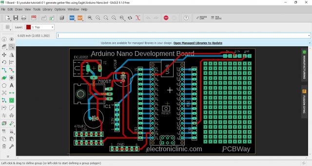
Open your PCB design. Click on the File menu > Open > Board, open the folder where your PCB file is saved.
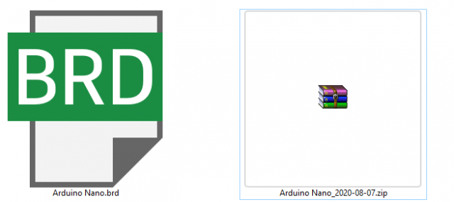
Download the Brd file:Arduino Nano
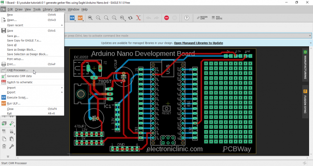
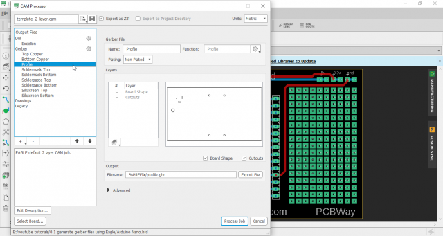
Double check all the connections before you generate PCB Gerber files, once you are satisfied with all the connections, click on the file menu and then click on the CAM Processor.
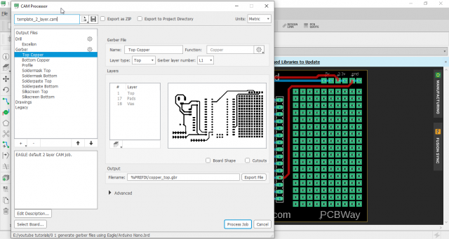
This will open the CAM Processor window as you can see in the picture given below.
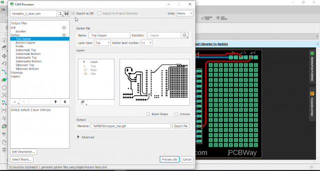
On the top you can see the Export as ZIP check box, check this box.
After checking the Export as ZIP box the next step is to click on the Profile available under the Gerber heading.
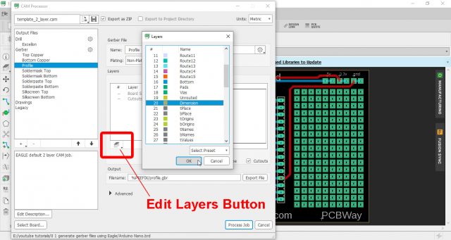
Now, the final step before you clicks on the Process Job button is to click on the Edit Layers.
This will open the Layers window, scroll down and select the dimensions layer and add it by clicking on the OK button. Now you can click on the Process job to generate PCB Gerber Files.
This will generate the ZIP folder consisting of the all the required PCB Gerber files.
You can right click on the ZIP folder and extract all the files, if in case you want to check what’s inside this ZIP folder. This is how easily you can generate PCB Gerber files using the Cadsoft Eagle software.
Online Gerber Files Viewer by PCBWay:
You can also use the Cadsoft Eagle software for viewing the Gerber files, but I recommend you should use the PCBWay Online Gerber Viewer.
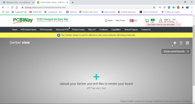
Let’s check our generated PCB Gerber files using the PCBWay Online Gerber viewer.
Search for the PCBWay online Gerber viewer.
Click on the PCBWay online Gerber viewer link.
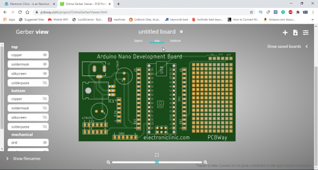
Simply drag and drop the zip folder that we just created. Or you can use the + button to add the zip folder. The time you add the zip folder, all the files are loaded. Click on the top to check the top side of the PCB.
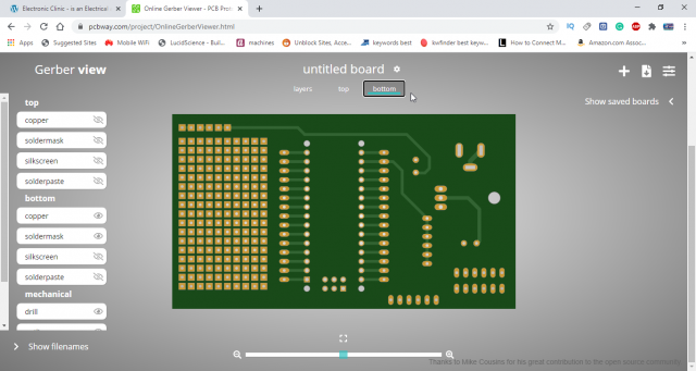
On the bottom to check the bottom side of the PCB.
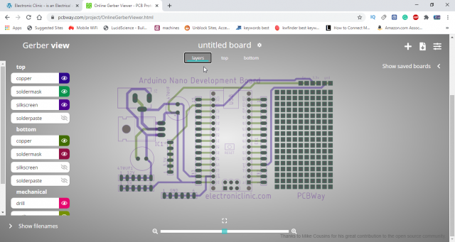
Click on the layers to check top and bottom sides copper, soldermask, silkscreen, and solderpaste, along with the mechanical stuff. You can easily make any layer visible and invisible by simply clicking on the eye icon next to every layer.
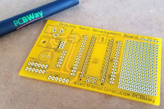
So, this is how easily Gerber files can be generated using the Eagle software. For the step by step procedure watch video given below. Finally, I uploaded the Gerber files on the PCBWay official website.
About the Sponsor of this project, PCBWay:
High quality & Only 24 Hours Build time
PCBWay is quite professional in the field of PCB manufacturing; you can try their services at extremely low prices, Only 5 dollars for 10 PCBs and 30 dollars in total for 20 PCBs assembly, besides this the new members also get a 5 Dollars bonus.
PCBWay is currently Celebrating 6th Anniversary offering Mid-Year Big Sale. I am really thankful to the PCBWay for continuously supporting my work by sending me such High-quality PCBs.
If you want to know more about the Gerber Files continue reading this article.
Why do we need to Generate PCB Gerber Files?
Only the PCB board layout file with the extension .brd is not enough to manufacture the PCBs. The PCBs manufacturing companies need the Gerber Files. The Gerber format is an open 2D binary vector image file format. It is the standard file used by printed circuit board (PCB) industry software to describe the printed circuit board images: copper layers, solder mask, legend, etc.
Gerber files should be inside a .rar or.zip archive with standard file extensions:
Extension Layer
pcbname.GTL Top Copper
pcbname.GTS Top Soldermask
pcbname.GTO Top Silkscreen
pcbname.GBL Bottom copper
pcbname.GBS Bottom Soldermask:
pcbname.GBO Bottom Silkscreen:
pcbname.TXT Drills
pcbname.GML/GKO *Board Outline:
Note: 4 layer board also need
pcbname.GL2 Inner Layer2
pcbname.GL3 Inner Layer3
Once the PCB layout is designed you will need to generate the Gerber files. Gerber is used in PCB fabrication data. PCBs are designed on specialized electronic design automation (EDA) or a computer-aided design (CAD) system e.g. Cadsoft Eagle and there are so many other Schematic and PCB designing softwares. The CAD systems output PCB fabrication data to allow fabrication of the PCB board. This data typically contains a Gerber file for each image layer (copper layers, solder mask, legend or silk…). Gerber is also the standard image input format for all bare board fabrication equipment needing image data, such as legend printers, photoplotters, direct imagers or automated optical inspection (AOI) machines and for viewing reference images in different departments. For assembly the fabrication data contains the solder paste layers and the central locations of components to create the stencil and place and bond the components.
Over the last few years there have been several attempts to replace Gerber by formats containing more information than just the layer image, e.g. netlist or component information. None of these attempts have been widely accepted within the electronics manufacturing industry, probably because the formats are complex. Gerber remains the most widely used data transfer format.
