PCB Printed Circuit Board Technology Fully Explained
Last Updated on September 9, 2021 by Engr. Shahzada Fahad
Table of Contents
PCB Printed Circuit Board:
PCB stands for printed circuit board are widely used in electronics in order to mount and create circuits on it. A PCB is used to interconnect all the electrical and electronic components together on a common board. In PCB all the components are connected internally so no wires are used.
A printed circuit board connect the electrical and electronic components on a common board. A PCB is a thin board made up of fiber glass, composite epoxy or other laminate material. Conductive pathways are etched or printed on to board connecting different components on the PCBs such as resistors, transistors, and integrated circuits. All the components are internally connected and we do not need any extra wire to connect the components all the components are surface mounted.

PCB is considered as back bone of every electronics. In today world every electronic device contains PCB and it acts as base for other components. For example in our mobile System on chip is on PCB similarly memory is also on PCB. PCB is made up of fiber glass and copper sheet. These are the two main elements. We use drill for connection and mounting of the PCB. PCB has copper tracks to connect the holes where the various components are located.
Need of PCB(Printed Circuit Board):
Before the invention of PCB we make use of cable to connect various components but after invention of PCB these cables were replaced by copper traces. The need of the pcb occur because it reduce the complexity and also help to make easy connection. PCB save a lot of space also reduce the overall board weight. It helps us to easily read the connection one component to the other component. It allows clean construction and made mass production possible. It is easy to diagnose and repair because it consists of labels on the board. The designing of the PCB is more robust because a physical wire is more likely to break than a copper tracer. It has no loose connections or short circuits.
Material used for PCBs:
The conducting layer of the PCB printed circuit board is copper but the base material can be of epoxy glass or Teflon. Different materials are used for the fabrication of the printed circuit board.
FR4:
Most commonly used material in PCBs. It is glass reinforced epoxy laminate sheet. We used flame because it is flame and water resistant. It provides good strength to weight ratio.
PTFE (Teflon):
The best known PTFE based brand name is TEFLON offers temperature stability.
Aluminium:
Most common ceramic PCBs use aluminium having strong thermal dielectric with low thermal expansion.
Types of PCBs:
- Single layer PCB
- Double layer PCB
- Multi-layer PCB
- Rigid PCB
- Flexible PCB
Single layer PCB(Printed Circuit Board):
A single layer PCB is a single layer of base material or substrate in which one of the side of substrate is coated with copper which work as electric conductor on a single layer PCB only on one side components can be mounted. The substrate which is glass material or ER4 is basically nonconductive on which copper layer is mounted and it is single sided. It consists of electronic component only on one side. This type of PCB are used in calculators or power supply.
Double layer PCB(Printed Circuit Board):
A double layer PCB has a thin base layer of conductive material on both the sides of substrate. Holes are drilled on the board in order to allow the circuits of the first side to connect on the second side. It is usually in such cases where we want to avoid jumpers otherwise we will need extra wires due to which our circuitry will become bulky.This type of PCB are used in led lightning, automotive dashboards, amplifiers, and vending machines etc.

Multi-Layer PCB(Printed Circuit Board):
A multi-layer PCB have a series of three or double layered PCBs connected to each other. Such PCBs are mainly used for professional purposes such as GPS technology, satellite system, data storage, and file servers. This PCB consists of upper layer and bottom layer the substrate is used between them in order to avoid short circuiting. The advantage of the Multilayer pcb is that we can decrease the size of the circuitry. It enlarges the density and complexity of PCB design by adding extra layer beyond the top and bottom layer. Extra layers used for power planes and also decrease the level of electromagnetic interference

Rigid PCB(Printed Circuit Board):
A Rigid PCB is made up of solid substrate material in order to prevent the board from twisting and provide the circuit a longer life span. This PCB is used and manufactured on a large scale they are mainly used to design motherboards of laptops and desktops. A mother board is example of the Rigid PCB.
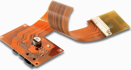
Flexible PCB(Printed Circuit Board):
A flexible PCB is made up of materials which can flex or move mainly plastic. This PCB costs more as they need to be printed on flexible materials. This field is still underdevelopment as there is need for proper material in order to create a proper functional PCB at lower cost. This type of PCB are used in LCD panels or smart watches.
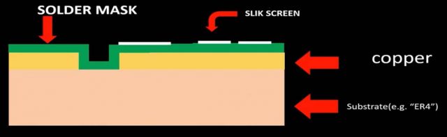
Layers of PCB(Printed Circuit Board):
In the picture we can see different types of layer:
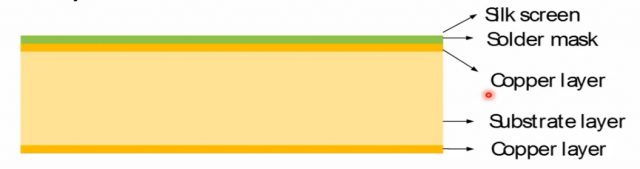
Now we will discuss each layer in detail:
Silk Screen:
This layer is basically nothing electrically it is used to indicating for placing component, logos and marks, information about components. Silk screen is present where we want to place the component. Colour is usually white but can be other colours also depending upon the PCB manufacturing process. Do not put the silk screen on the area that is going to soldered the silk screen will weaken the solder joint. It will helpful in the troubleshooting of the circuit.
In the above picture we can easily read that we are using 74AC14 IC and also we can see the different pins of the IC this is due to the silk screen. It is possible to make a circuit without silk screen.
Solder Mask Layer:
Protective layer: it protect copper layer from dust or other environmental influences and short circuit of traces. It also do nothing electrically but for the protection of the traces like wires or cables we have traces in them for the protection there is possibility of short circuit. The solder mass is made up of polymer. Solder mask basically work as a skin of the PCB(Printed Circuit Board).

Copper Layer:
The current flow through this layer usually it thickness is 1 oz which is equal to 35 micrometer or ¼ mil. The thickness of the pcb affects the price of the pcb.
1 mil = thousandth of an inch
1 mil = 0.025 mm
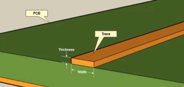
It does not cover complete surface of the pcb it consist of traces that we will use in the PCB. The copper layer connects different component together. The copper layer carry or transmit the electrical signal.
Substrate Layer:
It holds the component and traces and insulates them. The material which are used in it are FR4, Teflon and special polymers. They can withstand voltage and have insulation resistance. The substrate provides the strength to the PCB to prevent it from the breaking. In simple words we can say that the substrate is the skeleton of the PCB(Printed Circuit Board).
PCB designing Softwares:
Various types of softwares are used for designing the pcb such as:
- Fritzing
- Easy Eda
- Eagle auto disk
- Ki cad
- DS PCB
These are the softwares in which we can easily design our PCBs.
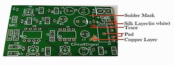
PADS in PCB:
Now we will discuss what the pad is and why we need to use them in our PCB(Printed Circuit Board) designs. So by the basic definition if you don’t know how the soldering of the components to the pcb board. We basically can connect our components on the pcb with the help of the path. These are the connection points of the components to the pcb surface. We have two types of the pad depending on the components that we are using for example if we are using through-hole components it is obvious that we want to usethrough-hole for example pads for the surface mount deviceswe need to justuse surface small pads in order toconnect them to the pcb surface.
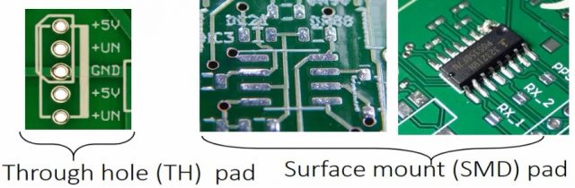
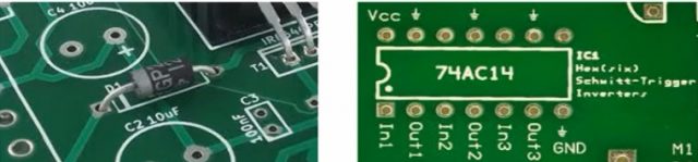
In these two pictures you can see we have surface mount devices. surface mount pad it the right hand side picture. These two pictures you can see that we are using the surface mount device and for the left-hand side you see that we are using through-hole pads instead of using surface mount pad and one important thing i have to mention is about the cost of just connecting the through-hole or super smart devices. If you are going to have a cheap pcb for example manufacturing of your circuit it may be good to use surface mount devices and surface mount pad but you know why because installation of the components on the PCB(Printed Circuit Board) with this technology is easier and cheaper but through-hole it will be little bit expensive because it requires drilling holes inside the all layers of the pcb. it is a little bit time consuming and expensive for the manufacturer. So if it is possible you may want to consider surface mount devices for your circuit instead of using through-hole technology but in some cases for example let’s say you have a high mechanical tensions and the tail multinational you may want to consider through hole. You know why because surface mount is not reliable and it is not trustable in high tensions and we do not want to consider surface mount for your devices. This is one of the reasons that for the connectors for example we want to use through-hole becausewe always connect wires to the board and they are exposed to the high mechanical tesnsions and for that reason we are using through-hole instead of surface mount for themost of the connectors in the PCB(Printed Circuit Board).
Component Placement on PCB:
The component placement on PCB sometimes it seems to be easy to place the components on the pcb to place the capacitors or IC. But it is not really that simple and it sometimes becomes really complicated and hard to just place the components, proper component placement can be manufacturability, visibility, and durability for your system. The circuit which is properly placed can be easy to manufacture, can be easy to troubleshoot, and has higher lifetime. Now let’s consider that you have a pcb that consist of analog sections, analog devices, digital devices, digital processor or power section.So one of the most important tips that you can have to do is that don’t mix them together. You know why because they have noise and interference to each other. For example let’s say you are mixing analog and digital sections in digital system we have one and zero.They are changing between the one and zero they have sharp rise and fall from zero to one and from one to zero. This sudden change can have noise inside the traces. For example let’s say sensitive analog devices having signals so if you mix them together they will do interference. They are going to have noise on the other section. So keep them a little bit away from each other. You may want to consider one of the corners for example for the analog the other corner for the digital. The other area for the power section and the power section is really important you know why because they are exposed to the higher currents inside the pcb and they can impose higher interference to their surrounding area so, keep them a little bit away from each other, this point must be kept in mind while designing the PCB(Printed Circuit Board).
Keep component away from heat generating parts like power switches as a designer before you are going to design it or assemble it you must know about the heat generating elements for example if you are working with power electronics for example you may want to consider the power switches like IGBTS or power MOSFET as a heat generating elements you have to pay attention to these elements or linear regulator. You know that you are just generating power and they are responsible for the increase of heat in the in the circuit.
Discover more from Electronic Clinic
Subscribe to get the latest posts sent to your email.