SR Latch and SR Flip Flop truth tables and Gates implementation
Last Updated on September 12, 2021 by Engr. Shahzada Fahad
Table of Contents
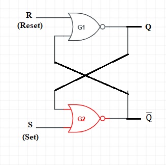
SR Latch using NOR gates:
sr flip flop:- Latch is basic storage element in which we store 0 or 1. Latch as name suggest it holds 0 or 1. In the circuit “R” stands for reset and “S” stand for set. Q and are the output of the latch. When the circuit will be reset Q value will be equal to 0 and when the circuit will be set the Q value will be equal to 1.
Case 1:
When the S =0 and R = 1 and we will study the Q and Q ̅ output
As we are using NOR gate and its truth table is:
| A | B | Output |
| 0 | 0 | 1 |
| 0 | 1 | 0 |
| 1 | 0 | 0 |
| 1 | 1 | 0 |
So we will use this truth table to understand the SR latch as when one of the input is 1 the output of the NOR gate will be 0. So when S = 0 and R =1 the output Q will be 0 because the input of NOR gate G1 is 1. The output of the G1 NOR gate will be given at the input of NO gate G2 which is 0 and as the S = 0 as both inputs of the NOR gate G2 are 0 so the output of G2 will be 1. So in Case 1 when S = 0, R = 1 then Q = 0 and Q ̅=1 Now to check whether this one bit is store in it or not we will remove the inputs. Both the inputs will be zero. As both the input of G2 are 0 so its output will be 1 and the output of G2 is connected with the input of G1 as one input of the G1 is 0 while the other input is 1 so the output of the G1 will be 0.
When S = 0, R = 0 then Q = 0 and Q ̅=1
Which shows that one bit is stored in it and it will work like a memory.
Case 2:
When S = 1, R = 0 then we will see that what will be the values of Q and Q ̅ output:
Now in this case the input of NOR gate G2 is 1 so when one of the input of NOR gate will be 1 its output will be 0 and as the output of G2 is connected with the input of G1, so both the inputs of G1 will be 1 due to which the output of the G1 will be 1. S = 1, R = 0 then the output will be Q = 1 and Q ̅=0
Now to check again whether the output is store in it we will remove the inputs such that S = 0 and R = 0 Now again one input of G2 is one so the output of G2 will be 0. As this output is connected with the G1 so both the input of G1 will be 0 and we will get 1 at the output of G1.
S = 0, R = 0 then the output will be Q = 1 and Q ̅=0
Which shows us that it worked like a memory and the bit is stored in it.
Case 3:
When S = 1, R = 1 then we will see that what will be the values of Q and Q ̅ output:
As one of the input of both NOR gate are 1 so whatever will be the other input we will get 0 at the output.
When S = 1, R = 1 then the output will be Q = 0 and Q ̅=0
Now to check whether the bit is store in it or not we will remove the inputs let us consider that the output of the G1 gate is zero as both the input are zero of the G2 so we will obtain 1 at the output of G2.
Now consider G2 output is 0 so both inputs of G1 will be 0 and we will obtain 1 at the output. It means that we have not change the inputs but there is change output which shows us that it is contradictory state.
So in the SR latch we will not use S =1 and R =1 state.
Truth table of SR latch:
Now we will draw truth table for SR latch:
| S | R | Q | Q ̅ |
| 0 | 0 | Previous state | |
| 0 | 1 | 0 | 1 |
| 1 | 0 | 1 | 0 |
| 1 | 1 | Not used |
SR latch using NAND gate:
In SR latch using NAND gate we will replace NOR gate with the NAND gate. The inputs are interchange in SR NOR latch we have reset in the upward gate and set in the lower gate. While in this circuit we are applying set to the upper NAND gate and reset to the lower NAND gate and Q and Q ̅ represents the output of the latch. The circuit will be set when the Q = 1 and the circuit will be reset when the Q = 0.
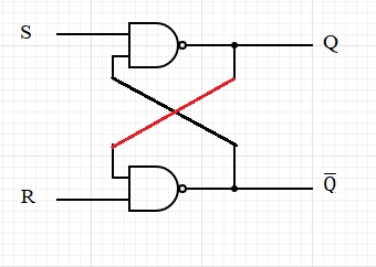
In order to understand the working of SR latch using NAND gate we will first draw the truth table for NAND gate which is:
| A | B | Output |
| 0 | 0 | 1 |
| 0 | 1 | 1 |
| 1 | 0 | 1 |
| 1 | 1 | 0 |
Now we will study different cases:
Case 1:
When S = 0 and R= 0 what will be the value of Q and Q ̅. From the above table we see that whenever the input to NAND gate is 0 we will get 1 at the output. As at G1 the input is 0 so we will obtain Q = 1 at the output. Similarly the input to G2 is also 0 so we will get 1 at the output. But this type of output is not true because Q and Q ̅ are complement of each other. So this state will not be used because both output cannot be 1 and it is undesirable. This type of situation occur in SR latch using NOR gate when the S and R value was 1.
When S = 0, R = 0 then the output will be Q = 1 and Q ̅=1
Case 2:
When S = 1, R = 0 then the output Q and Q ̅ will be:
As the input of G2 is 0 the output Q ̅=1 and when this output is feed to the input of G1. So both the input of G1 will be 1 and we will get 0 at the output.
When S = 1, R = 0 then the output will be Q = 0 and Q ̅=1.
Case 3:
When S = 0, R = 1 then the output Q and Q ̅ will be:
As the input of G1 is 0 so the output Q = 1 and as this output is feed to the input of G2. So both the input of G2 will be 1 and we will get 0 at the output.
When S = 0, R = 1 then the output will be Q = 1 and Q ̅=0.
Case 4:
When S = 1, R = 1 then the output Q and Q ̅ will be:
In this case the previous state to G1 input is 0 because Q ̅=0 and S =1 so as one input is 0 the output Q will be 1 and as this output is feed to the G2 and R=1 so both the input of G2 will be 1 and we get 0 at the output.
When S = 1, R = 1 then the output will be Q = 1 and Q ̅=0.
We will obtain the previous state and in this case the latch will act as memory by storing the previous state.
SR latch using NOR gate Truth table:
| S | R | Q | Q ̅ |
| 0 | 0 | Not used | |
| 0 | 1 | 1 | 0 |
| 1 | 0 | 0 | 1 |
| 1 | 1 | Previous state |
SR Flip Flop:
In the SR flip flop we will use the SR latch using NAND gate and two extra NAND gate will be used which are G3 and G4. The input to G3 and G4 will be S and R respectively and clock signal is applied to both gates which will be train of pulses.
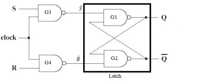
Operation of SR flip flop:
Let’s suppose the input to the latch is S ́ and R ́ and we will see the output value of the latch from the above table. S ́ is basically the output of NAND gate G3 whose one input is S and other is Clock.
(S ) ́= (S.clk) ̅
When we simplify this equation we will get:
(S ) ́= S ̅+ (clk) ̅ —– equation (1)
Similarly R ́ is basically the output of NAND gate G4 whose one input is R and other is Clock.
(R ) ́= (R.clk) ̅
(R ) ́= R ̅+ (clk) ̅ —– equation (2)
Case 1:
When the clock values will be 0 then the equation 1 and 2 will become:
(S ) ́= S ̅+ 0 ̅
(S ) ́= S ̅+ 1 = 1
So whatever the value of S ̅ we will get 1 at the output.
(R ) ́= R ̅+ 0 ̅
(R ) ́= R ̅+ 1 = 1
Case 2:
When clock value will be 1 then output would be:
(S ) ́= S ̅+ 1 ̅
(S ) ́= S ̅+ 0 = S ̅
(S ) ́ = S ̅
(R ) ́= R ̅+ 1 ̅
(R ) ́= R ̅+ 0 = R ̅
(R ) ́ = R ̅
When S = 0 and R=0
(S ) ́ = S ̅
(S ) ́ = 0 ̅
(S ) ́ = 1
(R ) ́ = R ̅
(R ) ́ = 0 ̅
(R ) ́ = 1
As we know that in latch when both inputs (S ) ́ = 1 and (R ) ́ = 1 then the output will be previous state.
Now if we consider S = 0 and R = 1
(S ) ́ = S ̅
(S ) ́ = 0 ̅
(S ) ́ = 1
(R ) ́ = R ̅
(R ) ́ = 1 ̅
(R ) ́ = 0
Then the output Q = 0 and (Q ) ́ = 1
Now when S =1 and R = 0
(S ) ́ = 0
(R ) ́ = 1
Then the output Q = 1 and (Q ) ́ = 0
Now when S = 1 and R = 1 then
(S ) ́ = 0
(R ) ́ = 0
Then this state will be invalid and we not use it as discuss above in latch case.
SR Flip Flop truth table:
| Clk | S | R | Q | Q ̅ |
| 0 | × | × | Previous state | |
| 1 | 0 | 0 | Previous state | |
| 1 | 0 | 1 | 0 | 1 |
| 1 | 1 | 0 | 1 | 0 |
| 1 | 1 | 1 | Invalid |
Characteristics equation for SR flip flop:
The present state of the flip flop will be represented by Qn and the next state will be represented by Q(n+1). Qn is basically the state which we feed to the input from the output.
| Clk | S | R | Qn+1 |
| 0 | × | × | |
| 1 | 0 | 0 | |
| 1 | 0 | 1 | 0 reset |
| 1 | 1 | 0 | 1 set |
| 1 | 1 | 1 | Invalid |
By using this table we will draw its characteristics table:
The inputs are S, R, and Qn act as inputs as we have three inputs there will be eight possibilities. To write the Qn+1 value we will look the table of the flip flop for the first case when the S and R both are 0 then the value in the table is Qn which is equal to 0. The same process will be used for other values.
| Qn | Sn | Rn | Qn+1 |
| 0 | 0 | 0 | 0 |
| 0 | 0 | 1 | 0 |
| 0 | 1 | 0 | 1 |
| 0 | 1 | 1 | × |
| 1 | 0 | 0 | 1 |
| 1 | 0 | 1 | 0 |
| 1 | 1 | 0 | 1 |
| 1 | 1 | 1 | × |
Now we will draw the k-map for the flip flop:
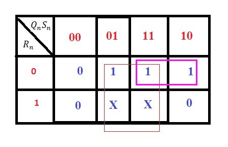
Where X represents don’t pair in the K-map table. We will make two group in which one group will consists of four element while other group consist of two elements.
For the first group above 1 is common which means Sn and in the second group again 1 is common which represents Qn and as it is in the first row so Rn will be o.
Q(n+1)= Sn + Qn (Rn ) ̅
So this is the procedure with the help of which we can draw the characteristics equation of the flip flop.
Discover more from Electronic Clinic
Subscribe to get the latest posts sent to your email.