Applications of Amplifiers, Inverting, Non-inverting, voltage follower, comparator, adder
Last Updated on July 4, 2022 by Engr. Shahzada Fahad
Table of Contents
Applications of Amplifiers:
An operational amplifier can be used for following purposes:
1). Inverting Amplifier
2). Non-Inverting Amplifier
3). Voltage Follower
4). Comparator
5). Adder or summer
6) Subtractor
7). Differentiator
8). Integrator
Treating operational amplifier as an ideal or a typical amplifier, now we elaborate on some of the key applications as mentioned above turn by turn:
Inverting Amplifier
Close loop configuration of an operational amplifier, in which input signal is applied on inverting input, is called inverting amplifier (remember the term close loop means re-connecting output with input through a feedback circuit) In other words, inverting amplifier is a close loop circuit of an operational amplifier, from which negative gain is received and which is detected through an external resistor. As amplifier name suggests, when a signal is applied on its inverting input, an inverted polarity amplified signal is received through its output (i.e. a difference of 180˚ or phase difference exists between the output received from such an amplifier and its input. As output voltage and input voltage are mutually 180˚ out of phase, that’s why such an amplifier is known as an inverted amplifier. Inverting amplifier is the most basic circuit of an operational amplifier, in which cumulative voltage gain is strengthened via application of negative feedback. As open loop voltage gain (AOL) is too high (i.e. even higher than 200,000) therefore, its application without any feedback is quite unsteady. Therefore, cumulative voltage gain requires to be strengthened via the application of negative feedback. Therefore, an inverting amplifier is also known as a negative scalar.
Figure 8.46 – inverting amplifier
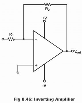
In figure 8.46 an inverting amplifier has been illustrated. According to the figure, some part of the amplifiers’ output has been provided a feedback via inverting input’s resistance R2. However, input signal has also been applied on inverting input via resistance R1, whereas non-inverting input is normally grounded. Remember that output signal is received between output terminal and ground of an operational amplifier.
Circuit Operation
For understanding the mechanism of an inverting amplifier, study the circuit shown in figure 8.47. Suppose that initial value of Vin is zero. As no potential difference exists between both input terminals during such a situation, therefore, output is also zero.
Figure 8.47- operation of an inverting amplifier
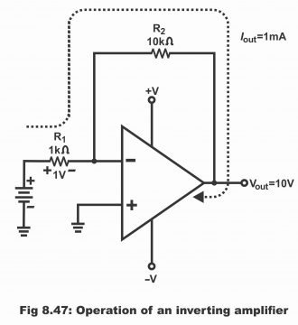
Now if Vin is gradually increased to +1V, in such a situation input starts getting 1V. However, output of an operational amplifier tries to keep inverting input on zero (remember that potential of non- inverting input is also zero). If the attempt succeeds, voltage drop parallel to R1 will be 1 volt, the polarity of which has been illustrated in the figure. 1mA current passes through it due to the presence of 1 volt parallel to 1KΩ. As no current penetrates into inverting input due to high input impedance, therefore this 1mA current should logically be received via output. As R1 and R2 are mutually arranged in a series or they are mutually configured, therefore current which passes through R1, should also pass through R2. Thus, when 1ma current transmits through R2, a drop of 10V will be received parallel to it. As potential of an inverting input is virtually equivalent to the ground (i.e. zero volt), therefore voltages which are received parallel to R2, same are the output voltages. Similarly, providing +1V on input, -10V on output is received. Thus, a gain value of -10 is received via an amplifiers’ output (negative sign along 10 reflects phase inversion) Remember that operational amplifiers’ output will supply 1mA current irrespective of R2 value. If a very high value of R2 has been chosen (or a very small value of R1 has been selected), output will saturate prior to reaching at its any suitable value. Through changing R2 value, it is possible to change output for any given input, thus changing R2 value will cause to change gain as well. However, gain can also be changed via changing R1 value. The relationship built up amongst R1, R2 and gain is as follows:
ACL = R2/R1
Inverting Negative Feedback
When a part of an amplifier’s output is returned/ supplied back on its input, it is called negative feedback. As voltage phase of an output differs from its input signal, therefore feedback signal opposes an inverse signal and tries to bring a decline in input signal. Apart from improving performance of an amplifier, feedback circuit also strengthens its voltage gain and mitigates distortion. Resultantly, a better frequency response is attained. Further, negative feedback eliminates output error, which results from input bias current, input offset current and input offset voltage. In figure 8.48, an inverting amplifier has been displayed. For keeping the circuit simple, power supply voltages have not been illustrated in it. According to the figure, negative input terminal of an operational amplifier has been connected with Vin via R1, while its positive terminal (i.e. non- inverting terminal) is grounded. When voltage Vin is supplied on amplifiers’ inverting terminal or negative input terminal, inverted polarity or phase voltage Vout are received from its output relative to Vin. That’s why such a circuit is called inverting amplifier. Input voltage Vin operate inverting input signal via resistor R1, by means of which inverting input voltage V2 are received. These input voltages get amplified via open loop gain and produce inverted output voltage. These output voltages are returned back OR feedback to input via resistor R2. As output is 180 ˚out of phase with respect to input, therefore the feedback input receives, is negative feedback. In other words, an inverted signal is always received on output with respect to its input.
Figure 8.48 – the inverting amplifier
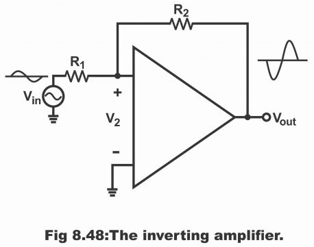
How can this negative feedback strengthens cumulative voltage gain? It can be understood in this way. That if open loop voltage gain (AOL) rises due to some reason, output voltage will increase and inverting input will also have more feedback. These inverted feedback voltages received on input reduce V2. Thus, V2 will experience a decline despite an increase in AOL. And thus, very little increase occurs in final output compared to an increase in output without negative feedback. Thus, the total value of an increase in output voltage is so small, that it is often ignored.
When voltages on an inverting input are positive, Vout starts moving towards negative side. As these negative voltage feedbacks are applied on inverting input via resistor R2, therefore these voltages strive to abolish changes taking place in Vin. In fact, feedback signal cannot totally eliminate an input signal, because if such a phenomenon becomes possible, we will not be able to get any feedback signal. However, in spite of this, feedback signal minimizes the impact of an input signal to a great extent. Remember that voltages on an operational amplifiers’ inverting input are practically zero no matter what ever occurs in Vin. This task is performed by feedback voltage.
Virtual Ground
Virtual ground is such a point on circuit which is located on ground potential (i.e. zero volts), however it is not connected to the ground. In figure 3.49, its three examples have been shown. In every condition, point A is on zero volts. However, it is isolated from the ground. The determination of voltage on point A is done via V1, V2 and resistor R1 and R2. If a volt meter is fitted between point A and ground, the volt meter will present a zero reading, though point A is isolated from the ground. Similarly, in case of amplifier Vi and Vout and resistors R1 and R2 keep the voltage of inverting input on zero volt as is clear in the figure 8.50. That’s the reason inverting input of an operational amplifier is considered as a virtual ground.
Figure 8.49
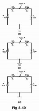
Thus, node which is at zero potential with respect to the ground, however mechanically not grounded, is called a virtual ground. Two types of grounds are normally used in electronic circuits. First type is called mechanical ground. Under this method, a node is connected with ground practically via a wire. Mechanical ground shorts node with the ground on all frequencies. Second type of ground is known as AC ground, which is normally denoted by means of a bypass capacitor. As capacitor’s capacitive reactance is low on high frequencies, therefore this type of ground operates only on high frequencies. Remember that both types of grounds facilitate /transmit current from node to ground.
Virtual ground differs from the two types of ground as mentioned above. No path is provided to the ground from node in this type of ground, despite this node potential remains zero. Remember that a virtual ground is only grounded for voltage but not for current i.e. it operates as a half ground. It has been denoted by dotted lines in figure 8.50. The analysis of an inverting amplifier and its related circuit can quite easily be done with the help of a virtual ground.
Figure 8.50 – the concept of a virtual ground: shorted to voltage but open to current
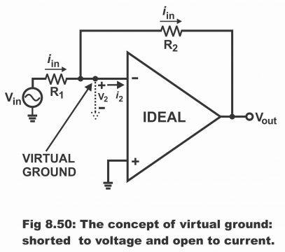
The concept of a virtual ground depends on an ideal amplifier (i.e. in order to consider the concept of a virtual ground, operational amplifier is considered being an ideal one) When an operational amplifier is treated as an ideal amplifier, in such a situation its open loop voltage gain and its input resistance is considered as being infinite. Thus, the following typical characteristics can be derived from an inverting amplifier.
1). As input resistance (Rin) is infinite, therefore, i2 value is zero
2). As open loop gain (AOL) is infinite, therefore, V2 value is zero
As the value of i2 is zero (as is clear from the picture), therefore current passing through the feedback resistor (R2), is equal to input. Further, as the value of V2 is zero, therefore the virtual ground as shown in the figure implies that inverting input function as a ground for the voltage, however for current it operates as an open (i.e. it does not function as a ground for current). It has thus become evident that virtual ground tends to be of an exceptional type. It works like half of a ground due to being short for the voltage and open to current. That’s the reason it has been expressed as dashed lines between inverting input and ground in the figure. The meaning of these dashed lines is that no current flows towards the ground.
Voltage Gain
In figure 8.51, a virtual ground has been shown on inverting input. In such a condition, right end of R1 is voltage ground. Thus, the value of input voltage will be as follows:
Vin = iin R1
Similarly, left end of R2 is voltage ground, thus the value of output voltage will be as below:
Vout = iin R2
Voltage gain results by dividing Vout by Vin, which equals the following simple equation.
Vout/Vin = iin R2/ iin R1 = ACL =R2/R1
Here, ACL means close loop gain. Due to negative feedback, close loop gain (ACL) is always less than open loop gain (AOL). Thus, close loop gain equals the mutual ratio between feedback resistance R2 and input resistance R1. For example, if R1 = 1KΩ and R2 = 50KΩ, the value of close loop gain will be 50. Due to heavy negative feedback, this close loop voltage gain tends to be quite stable. If AOL changes as a result of some change temperature, changes in supply voltage take place, by means of which ACL value still remains closer to 50.
Figure 8.51- inverting amplifiers has same current through both resistors
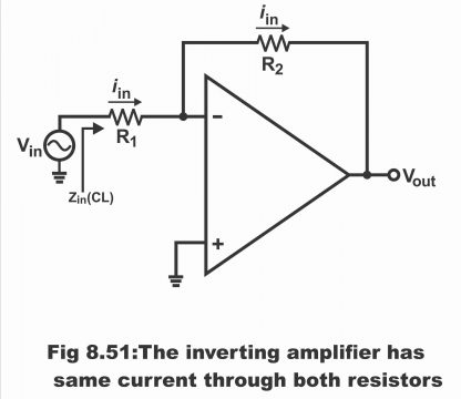
Explanation of Voltage Gain
In other words, current flows through R1 by means of input signal Vi. As voltage of an operational amplifier on an inverting input tends to be zero, therefore Vi must fully drop in R1, as result input current iin becomes as follows:
Iin= Vi/ R1 … 1
Output voltage (Vout) is inverted with respect to phase or polarity of input voltage (Vin). Due to these voltages, feedback current, which equals iin, transmits through feedback resistor R2 (i.e. same or symmetrical current transmits through R1 and R2). The left side of resistor R2 is at zero volts whereas the right side is on Vout. Thus, the value of feedback current is as below:
iin = VOUT/R2 … 2
The negative sign reflects that there is a phase difference of 180˚ between Vout and Vin. Thus, no current can penetrate into the inverting input of an operational amplifier, nor any current flows out from it.
Comparing equation 1 and 2,
Vi/Ri = Vout/ R2
Arranging the above equation,
Vout/Vin = – R2/R1
Remember that the ratio Vout/ Vin reflects close loop gain
Or ACL = AV = – R2/R1 … (where Av = voltage gain)
The negative sign shows that signal has become inverted. The above equation reveals that circuit gain can only be determined through the mutual ratio of R2 and R1.
Input and Output Impedance
In certain applications, a designer requires specific input impedance. One of the biggest advantages of inverting amplifiers is that it can be set on any specific or required input impedance quite easily. As right of R1 is a virtual ground, therefore the value of close loop input impedance will become equal to the following:
Z in(CL) = R1
This impedance is the left end impedance of R1, as can be seen from the figure. For example, if input impedance is 2KΩ and the required value of close gain voltage is 50, the designer can achieve this objective via keeping the value of R1 at 2KΩ and R2 value 100KΩ.
Remember that input impedance of an inverting amplifier never exceeds non – inverting amplifier or voltage follower. However, its output impedance, equals non- inverting amplifier (i.e. usually very low).
Zout (CL) = Zout/ AL
Here AL means loop gain.
Non –Inverting Amplifier
An amplifier on which input voltages are provided at non – inverting (or positive) terminal and no phase difference exists between its input and output (i.e. polarity of both input and output is same), is called non – inverting amplifier. Non –inverting amplifier is another basic circuit wherein overall voltage gain is stabilized via applying negative feedback. In such an amplifier, input impedance can be increased and output impedance can be decreased through negative feedback. In other words, non – inverting amplifier is actually such an ideal voltage amplifier, the input impedance of which is very low, while its voltage gain is balanced. Remember that gain received from the circuit can also continuously be adjusted between 1 to several hundreds.
Basic Circuit
In figure 8.52, basic circuit of a non – inverting amplifier has been illustrated. Input voltage Vin operate non – inverting input. These input voltages after having been amplified are received on output in the form of in-phase output voltage. Some part of the output voltage is fed back on input via voltage dividers (R1, R2). The voltages found parallel to R1 are the feedback voltages provided on inverting input. These feedback voltages are almost equal to input voltages. The difference found between V1 and V2 is very small due to a high open loop voltage gain. As feedback voltages are inverted to input voltages, thus we get a negative feedback.
Figure 8.52 – the non–inverting amplifier.

How does negative feedback stabilize overall voltage gain, it can be explained thus? If open loop gain (AOL) increases due to a certain reason, output voltages will increase. More voltages will be feedback on inverting input due to an increase in output voltages (i.e. more voltages will be fed back on inverting input). As these feedback voltages are inverse to input voltages, therefore overall input (V1-V2) decrease. Thus, in spite of an increase in AOL, final output experiences a very low increase due to a decrease in V1 and V2 (compared to an increase without negative feedback) (i.e. overall result being that increase in output voltage is very low)
Operation of Circuit
Suppose that +1V is supplied on Vin terminal of the circuit as has been shown in the figure 8.53, whereas the values of R1 and R2 are 1KΩ and 9KΩ respectively. For bringing potential of amplifiers’ inverting input to +1V, its output has to transmit 1mA current through R1. As input impedance of an operational amplifier is inordinately high, therefore no current transmits through inverting input. Thus, entire current passing through R1 also transmits through R2. If output supplies 1mA current which passes through total resistance 10KΩ, then output potential becomes +10V. Thus, supplying +1V input, +10V output is received and the gain value of the circuit is thus, 10. It has also be kept in mind that supplying positive potential on input with respect to the ground, results in a positive potential with respect to ground on output as well (i.e. both input and output of this circuit are positive) which means that both input and output of this circuit are In-Phase and due to this very reason, this amplifier is called a non – inverting amplifier.
Figure 8.53- Non- inverting amplifier
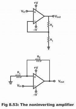
The close loop gains of a circuit can be determined via the mutual ratio of R1 and R2 (as feedback is provided from output to input, that’s why such a gain is known as close loop gain) If the value of R1 is dropped, operational amplifier will be forced to produce more current, so that an equivalent voltage drop is received. Higher output will be received as a result of higher current; thus, a higher gain will also be received. Increasing the value of R2, the same result can be achieved. The exact relation developed between the values and gain of R2 and R1, can be expressed with the help of following equation.
ACL = R1 + R2/R1 = 1+ R2/R1
Virtual Short
When we fix a piece of wire between two points of a circuit, the voltages of both these points are equal with respect to the ground. Moreover, wires provide a passage for the flow of current between these two points. This type of short (i.e. to short two points by fitting a wire between them) both for voltage and current is known as mechanical short.
Virtual short is different from a mechanical short. This type of short is used for the analysis of a non-inverting amplifier. Through virtual short, we can analyze a non–inverting amplifier and its related circuit quite quickly and easily.
In order to comprehend virtual short, following two characteristics of an ideal operational amplifier are used.
1). As the value of input resistance (Rin) is infinite, therefore both input currents are zero.
2). As open loop gain (AOL) is infinite, therefore values of V1 and V2 are zero.
In figure 8.54, a virtual short has been demonstrated between input terminals of an operational amplifier. Virtual short is short for voltage but open to current. Therefore, it has been illustrated in the figure via dashed lines, which means that no current can pass through it. Though, virtual short tends to be an ideal approximation, however when it is applied along a negative feedback, quite accurate answers can be obtained from it.
Figure 8.54 – a virtual short exists between the two op-amp inputs
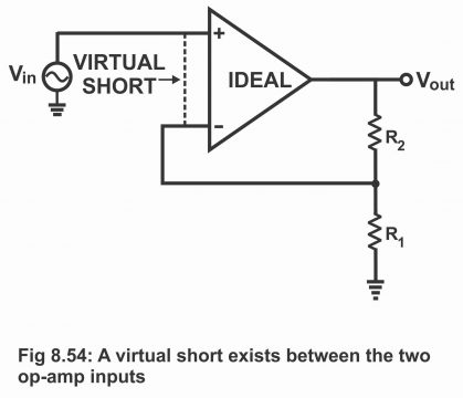
When we analyze a non –inverting amplifier or any other such circuit, we contemplate a virtual short between input terminals of an output amplifier. As long as operational amplifier operates in its linear region (i.e. so long as operational amplifier does not saturate positively or negatively), its open loop voltage gain is closer to infinity and a virtual circuit tends to exist between both its input terminals.
Another important point has been indoctrinated that by means of virtual short, inverting input voltage follow non- inverting voltages or they adopt according to it. That’s if non- inverting voltages increase or decrease, the inverting input voltages also increase or decrease immediately up to a symmetrical or same value. Thus, due to non- inverting input the inverting input increase or decreases to an equivalent value.
Voltage Gain
It may be assumed about the circuit shown in the figure 8.55 that a virtual short exist between its input terminals. In such a situation, virtual short means that input voltage appear parallel to R1 as has been shown in the figure (i.e. the voltages which appear parallel to R1 by means of a virtual short between both input terminals of an operational amplifier, are input voltages).
Thus, input voltages can be described as below:
Vin = i1 R1 … (1)
Figure 8.55-input voltages appears across R2 and same current flows through resistors
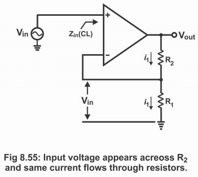
As no current flows through a virtual short (because virtual short is open for current) therefore an equal quantity of current passes through R2 as well (that’s the current which passes from R1, the same current also passes through R2). Therefore, output voltages (which are found parallel to the total of R1 and R2 on a series) in such a situation, can be expressed via the following equation:
Vout = i (R2 + R1) … (2)
Dividing equation 2 by the equation 1, we get voltage gain
Vout/Vin = i1 (R2 + R1)/ i1 R1
ACL = R2 + R1/R1
Or ACL = R2/R1 + 1 … (3)
If the afore – mentioned gain equation is looked at carefully, it becomes clear that there is no difference between the voltage gain of an inverting amplifier and non- inverting amplifier with the exception that 1 has been added with the resistance’s ratio (i.e. there is no difference in the voltage gain equations of both the amplifiers except +1), therefore it is very easy to be memorized.
Input and Output Impedance
The input impedance of a non – inverting amplifier is very high whereas its output impedance is very low. Thus, effective input impedance of a non- inverting amplifier is as follows:
Zin (eff)= AOL/ACL. Zin = AL Zin
Here, AL means loop gain and Zin means input impedance of an operational amplifier. Remember that Zin (eff) depends on loop gain. When the value of ACL is low, the value of Zin (eff) tends to be high. Effective output impedance can be expressed as follows:
Zout (eff) = Zout/ AL
Here Zout means output impedance of operational amplifier. By keeping loop gain value (AL) high, the value of Zout (eff) is kept low.
Voltage Follower
The circuit of an operational amplifier (non- inverting) the input impedance of which is very high and out impedance of which is low, and the voltage gain of which in case of a closed loop is unity (i.e. one), is known as voltage follower. In simple words, a closed loop non- inverting operational amplifier, the voltage gains of which is unity without phase reversal, is called voltage follower. As output voltages (Vout) of such an amplifier follow input voltages (Vin), that’s the reason it is called a voltage follower. This circuit reveals a very simple operation of an operational amplifier and it resembles an emitter follower (common collector amplifier of a transistor) circuit to a great extent. The only exception being that it works in a better manner. Remember that voltage follower circuit is not normally used for amplification due to its being unity gain. Rather, just like an emitter follower such a circuit is mostly used for impedance matching and isolation. That’s why voltage follower is often known as buffer or isolation amplifier as well.
In figure 8.56 (a) a voltage follower has been depicted. Input voltages (Vin) are provided on amplifiers’ positive input or non- inverting terminal whereas all output voltages (Vout) have been fed back directly on negative input terminal (or inverting input) (that’s output voltage feedback directly with the negative input). As output has been feedback on negative input, therefore it is called negative feedback. As feedback resistance is zero therefore, this negative feedback is usually maximum, due to which this type of circuit is very close to an ideal circuit. This negative feedback sounds quite weird in the beginning, because output helps in ascertaining the value of differential input (which tends to amplify in order to produce this output). As a virtual short exists between amplifier’s inputs, therefore in such a situation, output voltages are equal to input voltages i.e.
Vout = Vin
The situation of input voltage and output voltage being mutually equivalent means that value of closed loop voltage gain is unity or one i.e.
ACL =1
The mathematical method of ascertaining closed loop voltage gain is that if the value of R2 is considered zero, and value of R1 as being infinity, voltage follower gain can be determined by using the voltage gain equation of non- inverting amplifier.
ACL = R2/R1 +1 = 0/ + = 0+1= 1
Thus, voltage follower is a perfect follower circuit which generates output voltages which are exactly equal to input voltages. Besides, maximum negative feedback produces such closed loop input impedance, the value of which is quite high as compared to opened loop input impedance. Thus, closed loop impedance also ensues via this maximum negative feedback, the value of which is quite low as compared to opened loop output impedance. Thus, we almost get a complete technique for the purpose of converting a high impedance source to a low impedance source.
Figure 8.56 – (a). Voltage follower has unity gain and maximum bandwidth (b) voltage follower allows high-impedance to drive low-impedance load with no loss of voltage.

In figure (b) the concept has been elucidated wherein an input AC source consists of high input impedance R high while load has low impedance RLOW.
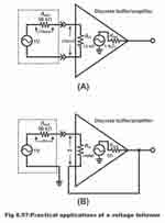
As negative feedback of a voltage follower is maximum (that’s 100% of output feedback on inverting input), therefore closed loop input impedance (Zin (CL) is high to an unbelievable extent whereas closed loop output impedance Zout (CL) is incredibly low. As a consequence, all input source voltages appear parallel to load resistor. Thus, input and output voltages of a voltage follower are considered identical for practical purposes. In figure 8.57, a practical application of a voltage follower has been shown for enlightenment. In figure (A) a signal source (output resistance of which is 50KΩ), has been connected with an amplifier (the input resistance of which is 15KΩ). If the value of an applied signal is 1V, only 230mV will appear on amplifier’s input while remaining 770mV drop parallel to the output resistance of signal source.
Figure 8.57 page 411 – Practical applications of a voltage follower

However, if the same signal source is connected with some specific amplifier voltage follower (input resistance of which is 100MΩ), as has been exemplified in the figure (B), the whole input signal will be received on amplifier’s input.
As output resistance of a voltage follower is very low, therefore any load fixed on its output, will receive full-fledged signal (that’s high input impedance of a voltage follower circuit enables it to receive even the weakest of signal from output without any signal loss. Further, output impedance of a voltage follower is so low, that this low impedance provides a full signal on loads)
Thus, a voltage follower, basically converts a high impedance voltage source to a low impedance voltage source and due to its this very characteristics, it is used as an ideal buffer amplifier for the purpose of interfacing (that’s for keeping both isolated) between high impedance sources and low impedance loads.
Comparator
A circuit which makes a comparison between two input signals or voltage levels is known as a comparator. In other words, if an operational amplifier is operated in an open looped mode (i.e. from output to input without any feedback), such a circuit is known as a voltage comparator. In figure 8.58, a comparator has been displayed. As there is no need to connect any additional external components along a comparator, therefore its circuit is extremely simple. Basically, a comparator’s output reveals that which of its two inputs is a high potential.
Figure 8.58

Suppose that two inputs (inverting and non- inverting) have been supplied on an operational amplifier’s circuit, while its output is the same, zero output is received in case both inputs are mutually equal. Now, if non- inverting input exceeds inverting input, comparator provides high output voltages. On the contrary, when non- inverting input is less compared to inverting input, comparator provides low output. In order to ascertain how does a comparator compare the two inputs signals and then provide output on this base, it is necessary to study the basic circuit of a comparator.
Working
We know that an operational amplifier is usually used in closed-loop mode (i.e. along with feedback), so that its voltage gain could be controlled accurately with the coordination of exterior components. It is never being used in open loop mode; because it’s extremely high open loop voltage saturates its output via any reasonable input signal. In order to understand how a comparator does compare two input signals and provides out on this base, the study of circuit shown in figure 8.59 is essential.
Figure 8.59 – Basic Op-Amp comparator circuit

When operational circuit is applied without any feedback, it works as a comparator as is vivid from figure 8.59. In situation of amplifiers’ inverting input being grounded, minimum input voltages are required for its saturation. Thus, if differential gain of an operational amplifier is AVOL, minimum differential voltages (Vd) required for the purpose of its saturation can be determined via the following formula:
Vd = Vsat/ AVOL
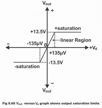
Suppose if power supply is , the output swings between +13.5 to -13.5 (that’s output fluctuates between )If the open loop gain of an operational amplifier is 105, in such a situation, the minimum input voltage, on which saturation starts, will be as follows:
Vd = V1-V2 = 13.5/105 = 13.5 … µV
That is, for saturating an operational amplifier (741C) +135µV in positive while -135µV in negative direction would be required. When the value of V1 exceeds V2 (135µV or greater) output saturates in positive direction on +13.5V. On the contrary, when the value of V2 exceeds V1 (135µV or more) output saturates on -13.5V in negative direction, as has been displayed vide figure 8.60. Thus, remember that comparator’s output consists of just two stable states i.e. negative saturation and positive saturation.
Figure 8.60 – Vout versus Vd graph shows output saturation limits.
There are several applications or uses of a comparator, out of which two of the uses have been illustrated in figure 8.61. The circuit shown in figure (A) is called zero crossing detectors, because when es cross waveform 0V, eout swing from one saturation level to another. When es are positive, the value of eout tends to be +13.5V. When the value of es is lower than zero volts (0V), the value of eout becomes -13.5V. When es values rise above 0V, eout value gets back to +13.5V.
The circuit shown in figure (B) is called a level detector. When input signal (ein) is lower than a DC reference level (EREF), this level detector immediately identifies the situation (i.e. level detector identifies or recognizes two different levels). DC reference (EREF) has been connected with positive input whereas ein has been supplied with negative input. As long as value of ein is high as compared to EREF, up to that point operational amplifier’s output keeps saturated on -13.5V. However, when ein value is lower than EREF, amplifiers’ output keeps saturated on +13.5V. The output of a level detector can also be used to operate an alarm or its output can be transferred to a computer as well, so that alarm could be turned on as level changes or the operation could be stopped through a computer.
Figure 8.61- comparator applications

Summing Amplifier
One of the advantages of an inverting amplifier is that it can provide output in the shape of a signal output through mutually summing up two or more than two analogue input signals. Thus, an amplifier which has the capacity of summing up two or more than two inputs is known as a summing amplifier. The output voltages of a summing or adder amplifier circuit are equal or proportionate to the algebraic sum of two or more than two input voltages (each of which is multiplied by a constant gain factor).
In figure 8.62 (a), a summing amplifier has been illustrated. For simplicity purposes, only two inputs have been shown in this circuit, however there may be a number of inputs. Such a circuit amplifies every input signal and gain of every input is expressed as a ratio of feedback resistance (RF) and proper input resistance e.g. as per figure (a) closed-loop voltage gains of two inputs are as follows:
ACL1 =RF/R1 and ACL2 = RF/R2
Summing circuit combines or adds all amplified input signals and converts it into a single output signal, which can algebraically be expressed as follows:
Vout = ACL1 V1+ACL2 V2
As inverting input is being virtually grounded, therefore input current i1 passing through R1 and input current i2 passing through R2 are equal to total input current i.e.
iin = i1+i2 =V1 / RF +V2/ R2
By means of a virtual ground, this total current generates output voltages after passing through feedback resistor, the values of which are as below:
Vout = (i1 + i2) RF = RF/R1 V1+ RF/R2 V2
It is clear from the above equation that each input voltage is multiplied with its input gain or channel gain and they are added or summed for getting total output i.e. Vout = Av (V1+V2). This principle applies on every number of inputs.
Figure 8.62-a, b, c – Summing Amplifier
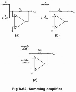
The values of resistances in some of the applications are the same, as displayed vide figure (b). In such a situation, closed loop voltage gain of every channel is unity (1) and output of such a circuit can be represented as follows:
Vout = V1 + V2 … +Vn
In figure © a mixer has been shown, which is an easy method of combining audio signals. The level of each input can be set via adjustable resistors as shown in the figure while the combined output volume can be adjusted via gain control. We can increase the signal value of V1 on output by means of reducing level 1 while by reducing level 2, we can increase V2 signal while both signals can be enhance via increasing gain.
Difference Amplifier
An amplifier which amplifies the difference existing between two input signals and provides an output in proportion to this difference is called difference amplifier. In other words, an amplifier which provides output equal to or in proportion to the difference between two input signals is known as a difference or Subtractor amplifier. A difference amplifier has been shown in figure 8.63.
Figure 8.63 – IC op-amp difference amplifier. With R3-R1 and R4=R2, the output voltage is Vo= R2 (VS2-VS1)/R1
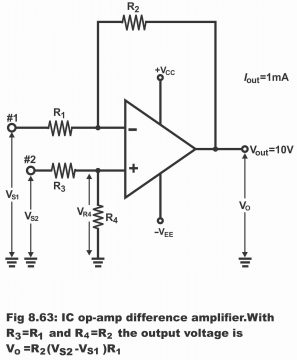
Difference amplifier comprises two inputs (i.e. inverting and non-inverting) and like other operational amplifier circuits, a practical amplifier also has a negative feedback. As inputs are supplied on inverting and non- inverting terminals of a difference amplifier circuit, therefore this type of amplifier is a combination or collection of both an inverting and non –inverting amplifiers. If input terminal 2 is grounded, the circuit operates as an inverting amplifier. Signal VS2 provides V4 getting divided parallel to resistor R3 and R4 which are received on non- inverting input of the operational amplifier. If terminal 1 is grounded, R1 and R2 operate as feedback components of non- inverting input of an operational amplifier. Thus, voltage V4 amplify as an input provided on a non – inverting amplifier. When VS2 value is zero, i.e. VS2 = 0, the value of first output will then be:
V01 = -R2/R1 x VS1
When VS1 value is zero, then VR4 and V02 values will be as follows:
VR4 = R4/ R3 +R4 x VS2
V02 = R1+R2 /R1 x VR4
By substituting value of VR4 in the above-mentioned equation,
V02 = R1+R2 /R1 x R4/R3x R4 x VS2
If R1 = R2 = R3 = R4, then
VO2 = R4/R1 x VS2 =R2/ R1 x VS2
The value of output signal in the presence of both the signals will be as follows:
V0 = V02+V01
= R2/R1 x VS2 – R2/R1 x VS1
=R2/R1 x (VS2-VS1)
Or V0 = Av (VS2-VS1)
Here Av means voltage gain and its value is equivalent to R1 and R2. It is obvious from the above equation that each input voltage has been multiplied by its input gain and the resulting total output equals to the difference between the two. Suppose that R1=R2, then the value of output voltage would be as follows:
V0= (VS2 – VS1) = Difference of the two-input ratio
Next Topic: Introduction to the 741 OP AMP
Previous Topic: Different Types of OP AMP Parameters
For electronics and programming-related projects visit my YouTube channel.
Discover more from Electronic Clinic
Subscribe to get the latest posts sent to your email.


Is this fig 4.48 correct. It shows inverted output but signal is applied to the non inverting input ?