Different Types of OP AMP Parameters
Last Updated on June 30, 2022 by Engr. Shahzada Fahad
Table of Contents
OP-AMP Operational Amplifier Parameters:
Different parameters or constants of an operational amplifier are as follows:
Input Offset Voltage Op AMP Parameter
When both inputs of an ideally operational amplifier are zero, in such a situation they produce zero volts (i.e. when both inputs of an ideal amplifier are zero, its output should also be zero at that time). However, very low DC voltages are received on output without the provision of a differential input voltage on a practical operational amplifier (i.e. even when no voltages are provided on a practical amplifier’s input, even then very low dc voltages generate on its output. The reason behind these low output voltages is the slight difference in input stages’ base to emitter voltages, as has been shown in figure 8.37. Due to the slight difference in Q1 and Q2 base to emitter voltages, little difference occurs in collector current despite an equivalent collector resistance. As a consequence, non-zero value voltage (Vout) is received on output. The slightest difference in voltages due to high gain is received in an amplified form on output.
Figure 8.37 Illustration of input offset voltages (Vos).
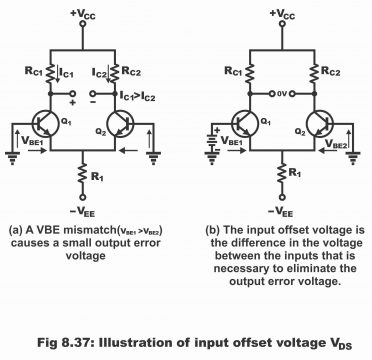
These voltages received on output can also be brought back to zero value through applying an offset voltage on input. Thus, input offset voltages (Vos) are differential dc voltages which are applied on input, so that output could be reverted back to zero value. In other words, input offset voltage is the difference of voltages in inputs, which is required to forcefully bring back output to zero. Vos has been clarified in figure (b). The value of input offset voltage ranges between 2mV to 4mV. However, in an ideal situation, its value is zero as shown in figure (b).
Input Bias Current Op AMP Parameter
Input bias current is a dc current, which is required by amplifiers’ inputs for operating the first stage of an amplifier in a befitting manner. Input bias current is equal to the average value of both of the input currents and it is expressed with the help of following formula:
IBIAS = I1 + I2/ 2
The concept of input currents has been shown in figure 8.38
Figure 8.38 – input bias current is the average of the two op-amp input currents
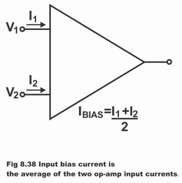
In other words, when the output of an operational amplifier is zero, some current transmits either inward or outward from the input terminal, which is equal to the average value of both input currents. It is known as input bias current. As these current changes due to fluctuations in temperature, therefore it can be a cause of destabilizing the circuit. Its value is usually less than one microampere. Remember that circuit will be more balanced if the value of the input bias current is lower.
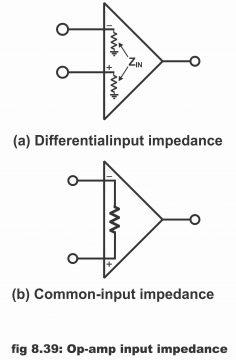
Figure 8.39 – op-amp input impedance
Input Impedance and Output Impedance Op AMP Parameter
The input impedance of an operational amplifier can be described by means of the following two methods.
1). Differential Input Impedance
2). Common-Mode Input Impedance
Differential input impedance is the resistance between inverting and non-inverting inputs, which is being displayed vide figure
8.39 (a). The measurement of differential impedance is done via ascertaining changes in bias current as a result of variations in differential input voltage.
Common mode input impedance is the resistance between each input and ground and it is measured via ascertaining changes in bias current due to variations in common-mode input voltage. In figure (b), common-mode input impedance has been shown. Remember that details of input impedance have been provided on the operational amplifier’s datasheet. Normally, the higher the input impedance, the better an operational amplifier works. The common input impedance value is greater than 1mega ohm.
On the contrary, the total resistance between the output terminal and ground of an operational amplifier is called its output impedance. Its value is extremely small (i.e. 75-150 ohm), because the lower the output impedance, the better an amplifier works. Output impedance has been shown in figure 8.40
Figure 8.40 Op-Amp output resistances.

Input Offset Current Op AMP Parameter
The difference between input bias currents is called input offset currents (Ios)
i.e. Ios=|I1-I2|
When both input bias currents are mutually equal, output of an ideal operational amplifier will be zero. However, bias currents are never mutually equal in a practical operational amplifier and some difference is experienced between them. Its quantity is about 20 nano amperes or input offset value is quite low (normally 10 times lower) as compared to a bias current. In other words, in order to set output current at zero, either one of the inputs will need more than 2mA current.
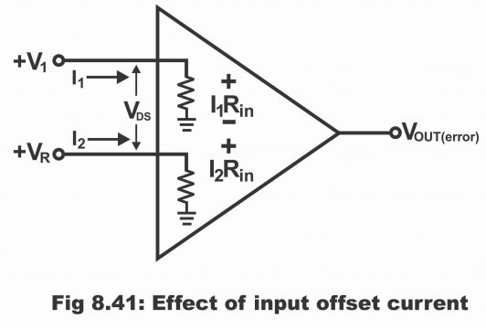
Offset current can be ignored in a number of applications, however amplifiers’ high gain, high input impedance, amplifiers’ input offset current should be minimum so far as possible. Because by means of difference in the currents as a result of high input resistance, a fair value of offset voltage generates, as has been shown in the figure 8.41
Input offset current leads to the production of following offset voltages
Figure 8.41-page effect of input offset current
Vos= I1 Rin-I2 Rin= (I1-I2) Rin
Vos=Ios Rin
The error which occurs as a result of input offset current (Ios), has been depicted on amplifier’s output as gain (As) after having been amplified i.e.
Vout (error) = As Ios Rin
Remember that change in offset current occurs as a result of fluctuations in temperature as well.
Common-Mode Rejection Ratio or CMRR Op AMP Parameter
The ratio between open-loop gain and common mode voltage gain is called common mode rejection ratio i.e.
CMRR = Al / Acn
It is normally described as decibels and its value is about 30000 or even higher. In other words, the capacity of rejecting common mode signals of an operational amplifier is known as CMRR. The infinite CMRR value means that when same signal is provided on both inputs, zero output results. Practically, achievement of an infinite value of CMRR is not possible; however, the CMRR value of a fine operational amplifier is surely very high.
When amplifier amplifies input signals, unnecessary noise and hue signals also penetrate into it, which mix with output after being amplified. Therefore, it is essential to remove these signals from amplifier for attaining best quality performance. Remember that a good amplifier can amplify desired signals by up to 100 times. It can reduce unnecessary common mode signals by 100 times. Therefore, the quantity of desired signals on output exceeds unnecessary signals by more than 10000 times. Thus, capability of an amplifier through which it amplifies a differential signal and stops/rejects common mode signal, can be expressed as a ratio, which is called CMRR. Thus, common mode rejection ratio is the ratio between differential gain and common mode gain. Through high CMRR value, an operational amplifier rejects these unwanted signals or interference from its output.
Slew Rate Op AMP Parameter
The maximum ratio of a change in an operational amplifiers’ output voltage is called slew rate of that operational amplifier. In other words, slew rate represents that characteristics of an operational amplifier through which it could be ascertained that how swiftly the output of an operational amplifier changes. It is denoted by SR. Slew rate can also be expressed as
SR = ∆ Vout/ ∆t
The unit of slew rate is volt per micro second. For example, 1V/µS means that a one-volt change occurs in output voltage per every micro second, irrespective of the level of change in input (i.e. output voltages of operational amplifier cannot change by more than one volt during one micro second time) In figure 8.42, the definition of slew rate has been clarified.
Figure 8.42 Illustrating definition of a slew rate

The range of a commercial amplifier’s slew rate is 0.25V/µS – 100V/µS. The unique slew rate of 741 operational amplifiers is 0.5V/µS. Thus, slew rate largely affects the AC operation of an operational amplifier due to which, in case of AC, amplifier operates in a finite mode on higher frequencies (i.e. in situation of high input signal, slew rate sets a limit for an operational amplifier, by means of which its output voltages cannot change so rapidly). Slew rate depends on the high frequency response of different amplifier stages within an operational amplifier.
Frequency Response Op AMP Parameter
We know that open loop voltage gain (AVOL) of majority of operational amplifiers is extremely high. It is possible only on low signal frequencies where AVOL value is relatively stable. As soon as frequency increases, AVOL declines immediately. On extremely high frequencies, its value becomes very low.
In figure 8.43, frequency response of a particular operational amplifier has been shown, which forms as a result of comparison between AVOL and frequency “f”. AVOL has been shown both in the form an absolute gain as well as decibels. The curve reveals that the value of AVOL remains constant at 100,000 (or 100dB) for frequencies ranging between 0 Hertz to 10,000 Hertz. In situation of a higher frequency than 10,000 AVOL start declining very quickly. A -3dB point has been shown on 10HZ. This is called high frequency cut-off point of an operational amplifier. It is also known as an open loop bandwidth (BWOL) of an operational amplifier. The value of open loop bandwidth of this operational amplifier is 10HZ in the figure (i.e. BWOL = 10 HZ). (Remember that bandwidth value for specific 741 operational amplifiers is 10HZ). After cut-off point, increases in voltage gain frequency leads to a reduction of at a rate of -20dB per decade.
Figure 8.43
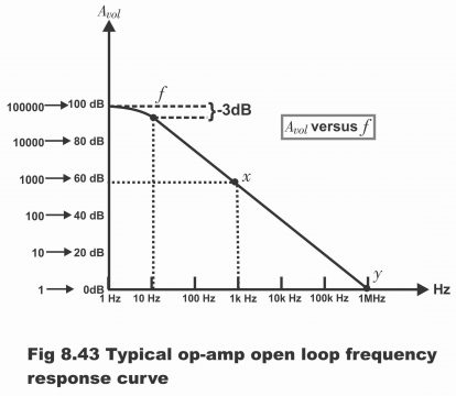
Unity gain bandwidth can be defined as a frequency on which the value of open loop voltage gain becomes one or unity. According to the figure, this frequency is 1MHZ, as can be seen via point y. Unity gain frequency or unity gain bandwidth is elaborated in the data sheets of an operational amplifier, so that amplifier is not used beyond that limit.
As compared to an open loop gain, close loop gain (ACL) relatively remains constant on wider frequency range. Close loop bandwidth (BWCL) refers to the frequency range at which ACL is relatively constant. A direct relation exists between BWCL and BWOL, which is as under:
(ACL) (BWCL) = AVOL BWOL = Gain – Bandwidth
It reflects from the relation that product of gain and bandwidth is constant, irrespective of whether the operational amplifier has been operating in open loop or close loop. As the values of AVOL and BWOL are normally being provided in the operational amplifiers data sheet, therefore BWCL value can be ascertained on any ACL desired value. When this relation is required to be applied, the absolute ACL value and low frequency value of AVOL are considered for the purpose. In short, circuit bandwidth will increase through the application of negative feedback and higher bandwidth can be achieved via lowering ACL. As soon as higher ACL values are used, circuit bandwidth declines.
Maximum Peak to Peak Output or MPP Op AMP Parameter
MPP value of an amplifier refers to its maximum peak to peak output. In other words, the peak to peak maximum output value which can produce an amplifier is called MPP. As output of an amplifier during an ideal situation is zero, however ac output voltages keep swinging between positive and negative values (i.e. such ac voltages are found on output, which are positive one moment and on other moment, they are negative. Consequently, zero output is received) As compared to output resistance (Rout), the value of load resistance is quite high. As a result, output voltages swing (increase or decrease) almost in coordination with supply voltages. For instance, if the value of VCC is +15V and VEE -15 volts, MPP ideal value in situation of 10 Kilo ohm resistance will be 30V.
In case of a practical or non-ideal operational amplifier, as some voltage drop occurs in the final stage of an operational amplifier, therefore its output cannot swing all the time according to the value of amplifier’s supply voltage. Moreover, when load resistance value does not exceed compared to Rout, some amplified voltage drop occurs parallel to Rout, therefore final output voltages become less as compared to an ideal situation.
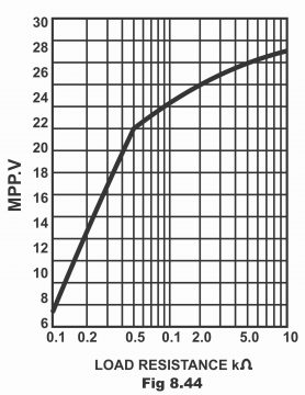
In figure 8.44, curves drawn between MPP and different values of load resistance of a 741C type operational amplifier have been
shown, which are drawn on supply voltage values. It is clear from the figure that at 10Ω value of R1, MPP value will be about 27V (though its value in an ideal situation is 30V). It means that output tends to saturate at +13.5 V and -13.5V. Remember that MPP also reduces as a result of a decrease in load resistance (as is evident from the figure)
Figure 8.44 – load resistance kΩ
Short Circuit Output Current Op AMP Parameter
In some of the applications, an operational amplifier drives a type of load resistance the value of which is zero. In such a situation, it is necessary to ascertain the value of short circuit output current. It is the maximum output current, which can be produced by an operational amplifier (i.e. maximum output current generated by an operational amplifier is referred to as its short circuit output current) Its value has been provided on amplifiers’ data sheet. According to 741C operational amplifier’s data sheet, its short circuit output current value is 25mA. When low value (i.e. lower than 75 ohm) load resistors are being used, maximum output voltages are not possible to be received, because in such a situation voltage (which is equal to the product of current and resistance) cannot exceed past 25mA times of the load resistance (i.e. decreasing the current value, lower voltage value obtainable via multiplying resistance and current, is achieved)
Common Mode Input Voltage Range Op AMP Parameter
There is a specific voltage range for the operation of an operational amplifier, through operating within which, a distortion less output can be received (i.e. all operational amplifiers have classification with respect to operating voltage regions as well). Therefore, common mode input voltage range is such a range of an operational amplifiers’ voltage, using which output can be produced without any kind of distortion or clipping. The value of common mode input voltage ranges of several operational amplifiers is , when DC supply voltages being provided on both inputs.
Open Loop Gain Op AMP Parameter
The voltage gains which is received from an amplifiers’ output back on its input without providing any kind of external feedback, is called open loop voltage gain (AOL). In simple words, voltage gain received from an operational amplifier without any kind of feedback is called its open loop voltage gain. Remember that open loop gain of a good operational amplifier tends to be on maximum side (i.e. 50,000-200,000). The amplifier will perform better the higher the value of gain. Gain is frequently expressed as an output volt provided on every mille volt of input. That’s a gain of 200,000 is expressed as 200V/mV. It means that if a change of 1mV occurs in input, a change of 200V will result in output. In other words, 200V/mV can also be described that change in output is 200,000 times greater as compared to input.
Power Bandwidth Op AMP Parameter
The highest frequency value (fmax) which can be amplified without any kind of distortion in slew rate is called power bandwidth or large signal bandwidth of that operational amplifier. Remember that if a value higher than this highest frequency value is desired to be amplified, in such a situation output voltage drop will occur in spite of the same peak. Moreover, slew rate distortion starts on any frequency in excess of this frequency (fin), which can be seen with the help of an oscilloscope.
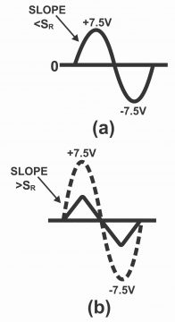
Distortion in any sine wave starts when initial slope of sine wave exceeds than slew rate (SR) of any operational amplifier as has been shown in figure 8.45 (remember that that the maximum ratio of a change in output voltage of an operational amplifier is called slew rate of that amplifier) In figure (a), initial slope of a sine wave has been shown. If initial slope of a sine wave is less as compared to the slew rate, operational amplifier produces sine wave output as shown in figure (a). On the contrary, if initial sign wave slope is larger than the slew rate, output received from the operational amplifier will comparatively be less and its shape will be triangular instead of being sinusoidal, as has been illustrated in figure (b).
Figure 8.45-(a) initial slope of a sine wave (b) distortion occurs if initial slope exceeds slew rate
As slew rate represents the fastest response of an operational amplifier, therefore complete details about slew rate are always mentioned in the datasheet of an operational amplifier, because quantity limits the large signal response of an operational amplifier. If output sine wave is very small, or its frequency is very low, then no slew issue arises. However, when signal is extremely large and frequency is high, slew rate distorts output signal (i.e. distortion or clipping occurs in output signal).
Initial sine wave slope is depicted via Ss and its value is as follows:
Ss = 2πf Vp
Here f implies sine wave frequency and Vp means sine wave peak value. In order to avoid slew rate distortion of a sine wave, SS
should either be equal to or lower than SR. When both are equal, in such a situation
SR = SS = 2πfVp
If above-mentioned equation is solved for f, the formula will become as follows:
fmax= SR/ 2πVP
Here fmax means the maximum frequency without any distortion or power bandwidth, which can be amplified. SR means sew rate and VP means peak value of output sine wave of an operational amplifier.
Next Topic: Applications of Amplifiers
Previous Topic: Operational amplifier OP AMP Introduction
For electronics and programming-related projects visit my YouTube channel.
Discover more from Electronic Clinic
Subscribe to get the latest posts sent to your email.
