BCD Encoder circuit diagram and truth table in digital electronics
Last Updated on November 12, 2022 by Engr. Shahzada Fahad
Table of Contents
BCD Encoder
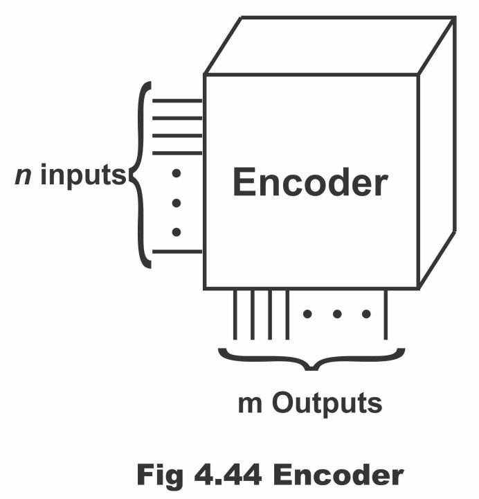
BCD Encoder circuit diagram and truth table in digital electronics- An encoder is a digital or logic circuit, which converts a decimal or octal input to a binary output. In other words, a logic circuit that operates exactly inversely with respect to a decoder and which converts non–binary numbers (i.e. decimal or octal numbers) to binary numbers, is called an encoder. As an encoder converts an active input signal to a coded output signal (i.e. one or more than one input is applied on it and it produces a binary output code greater than 1 – bit), it functions precisely oppositely to a decoder (because a decoder converts a specific code into a decimal one by means of reading or identifying it, whereas an encoder generates specific codes by itself and then converts them into binary). In figure 4.44, general diagram of an encoder has been illustrated. This diagram comprises “n” decimal input lines, of which only one line is active. The inner logic of the encoder converts this active input line to a binary “m” bit-coded binary outputs line. Output lines produce a binary code with respect to 2n input lines. Remember that encoders are constructed with OR gates and encoder ICs may be expounded as follows:
74147 … decimal to BCD encoder
74148 … octal to binary encoder
Figure 4.44 – encoder
In figure 4.45, a common decimal – to BCD encoder, which comprises four OR gates, has been illustrated. The switches mounted on it are just similar to the push buttons of a pocket calculator. The operational mechanism of this encoder is as follows:
Figure 4.45 – Decimal – to – BCD encoder
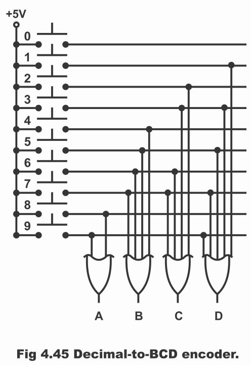
When push button 3, which represents decimal 3, is pressed, inputs of C and D OR gates become high (as an output of OR gate becomes high in case any of its input is high). Thus, the following BCD code is obtained on output.
ABCD = 0011
When push button 5 is pressed, inputs of B and D gates become 1 or high, while in such a scenario, inputs of A and C are low or zero. Resultantly, the following binary-coded output is received.
ABCD = 0101
Likewise, when switch 9 is pushed, then A and D gates are high whereas C and B gates are low. Thus, following output results.
ABCD = 1001
In figure 4.46, logic symbol of a decimal – to – BCD encoder whereas in figure 4.47 decimal digits (0 – 9) and its equivalent BCD code (or 8421) have been illustrated, with the help of which reciprocated relationship between BCD bit and decimal digits can be understood.
Figure 4.46 – logic symbol for a decimal – to – BCD encoder
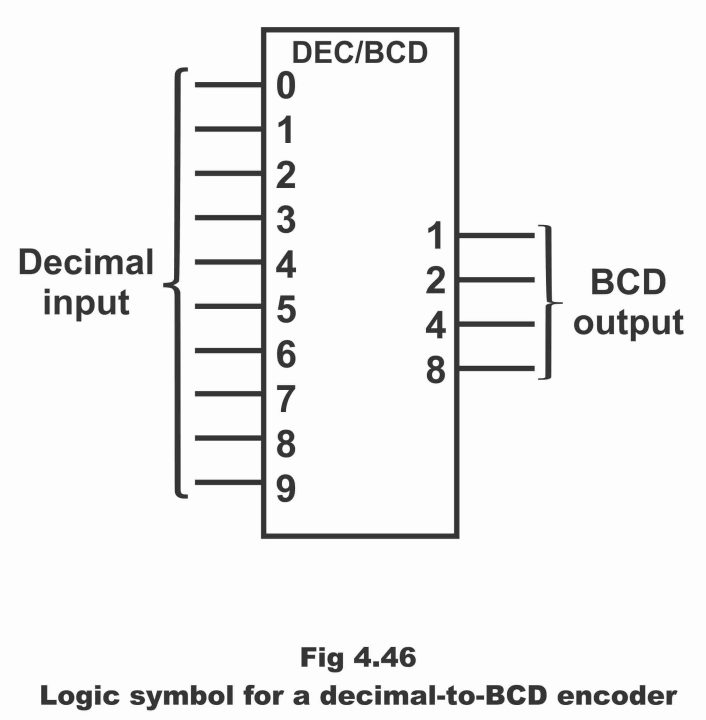
Figure 4.47: decimal to BCD encoder truth table
| Decimal Digits | BCD Code | |||
| 0 | A | B | C | D |
| 1 | 0 | 0 | 0 | 0 |
| 2 | 0 | 0 | 0 | 1 |
| 3 | 0 | 0 | 1 | 1 |
| 4 | 0 | 1 | 0 | 0 |
| 5 | 0 | 1 | 0 | 1 |
| 6 | 0 | 1 | 1 | 0 |
| 7 | 0 | 1 | 1 | 1 |
| 8 | 1 | 0 | 0 | 0 |
| 9 | 1 | 0 | 0 | 1 |
Decimal – to BCD Encoder
In figure 4.48, logic diagram of a basic BCD encoder has been illustrated, in which 0-digit input has not been displayed. This is because of the fact that in case of two inputs, entire BCD outputs are low. The operational mechanism of this type of circuit is as follows:
When any one of the decimal digits lines is high, then appropriate output levels result on four BCD output lines. For example, if line number 9 is high (assuming that all other input lines are low), then A0 and A3 output become high, whereas A1 and A2 output treads low. Consequently, 1001 BCD code is obtained for decimal 9.
Figure 4.48 – basic logic diagram of a decimal – to – BCD encoder. A 0-digit input is not needed because the BCD outputs are all low. When there are no high inputs.
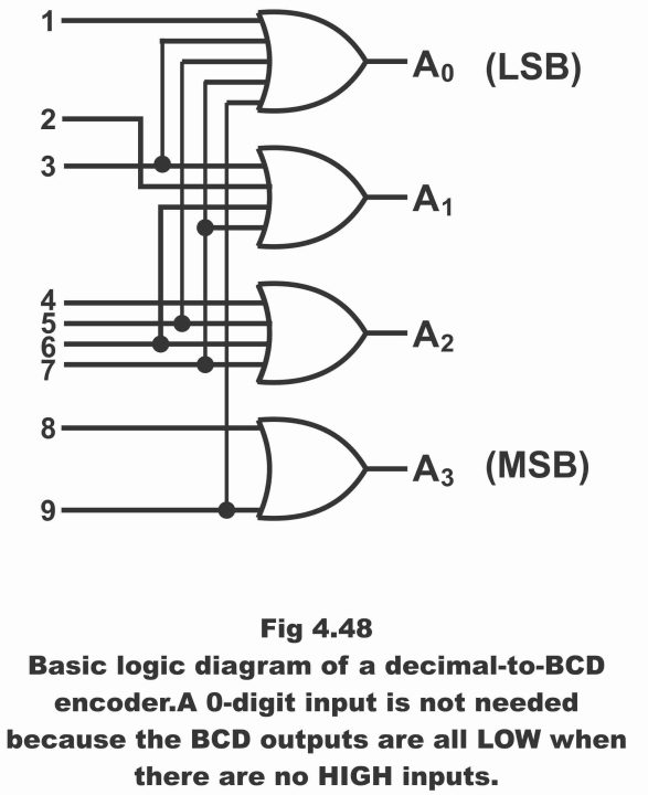
When line No. 1 is high, only A0 line is high whereas rest of the lines are low. Thus, a 0001 BCD code (i.e. 0001 = A0 A1 A2 A3) is obtained on output.
Similarly, when line No. 5 is high, then A0 and A2 lines are high whereas A1 and A3 lines are low. Consequently, BCD code is obtained in 0101 form, which is obviously equivalent to decimal 5.
74147 Encoder
74147 is a modern, state – of – the art 10- lines – decimal – to – 4 – lines – BCD encoder (i.e. it generates 4 – outputs from 10 inputs), which is mostly used as a priority encoder. It is an additional attribute of a 74147 encoder that apart from converting decimal inputs to BCD outputs, it encodes larger decimal input of two activated inputs. For example, if two inputs 3 and 6 are activated or turned to be high, in this case value of BCD output will be 0110, which represents decimal number 6.
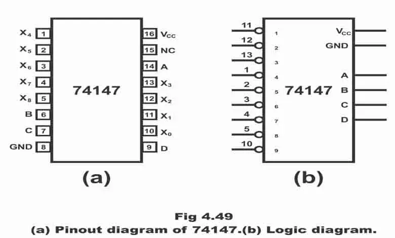
In figure 4.49 (a) pin diagram of a 74147 decimal – to – BCD encoder has been represented. It has decimal inputs from X1 through X9, which have been connected with pins 1 – 5 and pins 10 – 13. Pins 14, 6, 7 and 9 are BCD output pins or in other words, BCD output is received via pin number 14, 6, 7 and 9. Pin No. 13 is for supply, whereas pin No. 8 is ground. The word NC is written on pin No. 15, which implies “no connection” (that’s this particular pin is not used). In figure (b), logic diagram of 74147 has been denoted. The bubble sign or round circles along inputs and outputs reflect active low inputs and outputs (which suggests that when these pins are connected to the ground or GND, they tend to activate, which results in low output. In other words, input for which the code is desired to be generated, is essential that its input line be kept low. This function is called “active low input” or it may also be described as input being active low. In a similar manner, output may also be called “active low” and for elaborating this point on 74147 – IC, bubbles have been sketched)
Figure 4.49 (a). pinout diagram of 74147 (b). logic diagram
Operation
In figure 4.50, operation of 741497 encoder has been elaborated. Its detail is as under:
- When all inputs (X1 through X9) are high, in such a situation, all outputs are high (HHHH), the complement or inverse of which is (LLLL) (this can be possible only by means of mounting an inverter on outputs), which reflects decimal 0. This has been illustrated vide the first line of truth table.
- When only X9 input is low, ABCD output is high (HHHH) (as has been illustrated vide truth table). If these values of output are inverted with the help of an inverter (i.e. converted to HLLH or 1001), this output equals to 9 decimals.
- When only X8 input is low, ABCD output becomes LHHH, complement or inverse of which is equal to HLLL or 1000. This equals to decimal 8.
- When only X7 input is low, then values of ABCD will be HLLL or 1000, complement of which is (i.e. 0111) equals to decimal 7.
- Similarly, when input X1 is low (in which situation all other inputs are high), the ABCD output gate appears in the form of HHHL, the complement of which is LLLH. This represents BCD code equivalent to decimal 1 on output.
Figure 4.50 – truth table
| Inputs | Outputs | |||||||||||
| X1 | X2 | X3 | X4 | X5 | X6 | X7 | X8 | X9 | A | B | C | D |
| H | H | H | H | H | H | H | H | H | H | H | H | H |
| X | X | X | X | X | X | X | X | L | L | H | H | L |
| X | X | X | X | X | X | X | L | H | L | H | H | H |
| X | X | X | X | X | X | L | H | H | H | L | L | L |
| X | X | X | X | X | H | H | H | H | H | L | L | H |
| X | X | X | X | L | H | H | H | H | H | L | H | L |
| X | X | X | L | H | H | H | H | H | H | L | H | H |
| X | X | L | H | H | H | H | H | H | H | H | L | H |
| L | H | H | H | H | H | H | H | H | H | H | H | L |
However, it must be remembered that zero output is attained when none of the input is low, in other words when all inputs are high. In this case, all outputs also tend to be high (i.e. all LEDs are high). Therefore, all LEDs ae mounted in a reversed state or common anode state. As such, when an LED does not irradiate, it signifies that a state of 0000 has developed on the output (i.e. the BCD code value on input is decimal zero while on output it is 0000).
We know that 74147 is a priority encoder because it prioritizes the highest input value. The process of priority has been explained via a truth table given in figure 4.50. In case all inputs (X1 – X9) turn low at a time, only the highest input X9 encodes from amongst all these inputs, through which LHHL output is received. In other words, input X9 has priority over the rest of the inputs. When X9 is high, the largest input X8 gets priority owing to the fact that all other inputs are low. Thus, input encodes and it is received on output. If its truth table is studied cautiously, it becomes clear that the highest active low input (X0 – X9) always gains priority, which controls the function of encoding.
Previous Topic: seven segment display truth table and circuit diagram
Next Topic: Working Of Diode Rom with Gray Code and Circuit Diagram
For electronics and programming-related projects visit my YouTube channel.
Discover more from Electronic Clinic
Subscribe to get the latest posts sent to your email.

Great post! The detailed explanation of the BCD encoder circuit diagram and the associated truth table really helped clarify the concepts for me. Thanks for making it so easy to understand!