Working Of Diode Rom with Gray Code and Circuit Diagram
Last Updated on November 13, 2022 by Engr. Shahzada Fahad
Table of Contents
Read-only Memory
Working Of Diode Rom with Gray Code and Circuit Diagram- Read-only memory or a memory that can only be read (which is shortly known as ROM) is a kind of IC that can store thousands of binary numbers (which reproduce computers’ instructions and other enduring data). The best example of fixed data is the information that is present on an arithmetic table and which cannot be modified. As arithmetic data cannot be altered, therefore, it can be stored on a ROM.
ROM is the simplest and cheapest form of memory (remember by memory we mean a device that can store binary data for a longer or shorter period of time (for a better understanding of memory in detail, read out chapter 9). In other words, read-only memory (ROM) is a form of memory, wherein data can be stored either on a fixed basis or a semi-fixed basis. Data can only be read from a ROM and neither its data can be transformed without the application of some definite tool nor a new data can be feed onto it (i.e. write option does not exist in ROM, and data preserved in a ROM is readable only from the memory)
Hence, ROM is a kind of memory, wherein data is stored everlastingly and which can be extracted as and when required. However, data stored on ROM cannot be replaced with other data. In other words, instructions, tables and conversions, and other important matters about the operation of some digital system e.g. computer etc. are stored in ROM in binary word form, which cannot be transformed subsequently. However, important information can be retrieved from memory anytime and it can be read or write as well.
Remember that data stored on a ROM remains stored or protected even when power is off (i.e. its memory does not get damaged even if power supply has turned off) that’s why ROM is also known as non-volatile memory. Computer manufacturers store programs according to the instructions and requirements of a computer user via ROM. Small ROMs are used in order to solve combinational logic problems (e.g. decoding). ROM is also called Mask Programmed ROM. As compared to other memories, ROMs are quite cheap, fast- paced and relatively a larger amount of data can possibly be stored on a ROM (as compared to a RAM). ROM is used only in high volume production, because its initial cost is high. Remember that ROM is extensively used in digital systems e.g. microprocessor systems. The designer of a system, at the time of programming has to bear in mind the requirements of the person who has to use this system. A read – only memory is a device, which comprises a decoder and OR gates inside a single IC package. The data stored on a ROM (which consists on tables, system log on programs, operation programs, character codes, machine language etc.) is repeated frequently on system application. For example, irrespective of the number of times a computer is turned on, distinct information about its operation and structure is displayed on monitor screen every time it is turned on, which does lose even when supply powers off. As data is being fixed or stored permanently during the manufacturing of a computer, therefore it is treated as a computer’s internal memory, which can be read only through a processor. ROMs of different types and qualities are available these days in the market.
Diode ROM
The ROM in which diodes are applied for the purpose of storing data is called diode ROM. Suppose, we want to build such an integrated circuit (IC), which can store binary numbers as has been shown via a table given in figure 4.51. The line, path or spot, where these numbers are desired to be stored, are known as addresses. Nibbles in the table represent binary numbers, whereas decimal numbers 0 – 9 are addresses where these binary numbers are required to be stored (remember that in day–to–day life, messages are always associated with certain addresses. In case message is available, however, the address of the sender is unknown, it will not be possible to deliver that message. Here, nibbles have been supposed to serve as a message whereas decimal numbers 0 – 7 as address)
Figure 4.51 – Diode ROM
| Address | Nibble |
| 0
1 2 3 4 5 6 7 |
0111
1000 1011 1100 0100 1001 0011 1110 |
Suppose we want to store 0111 on address 0, 1000 on address 1 and 1011 on address 2. For this purpose, wherever there is logic 1 on data or nibble given in the table, a diode is mounted over there. The process of storing nibbles given in the table has been explained vide figure 4.52, where every position of the rotary switch has been associated with an address.
Figure 4.52 – diode ROM
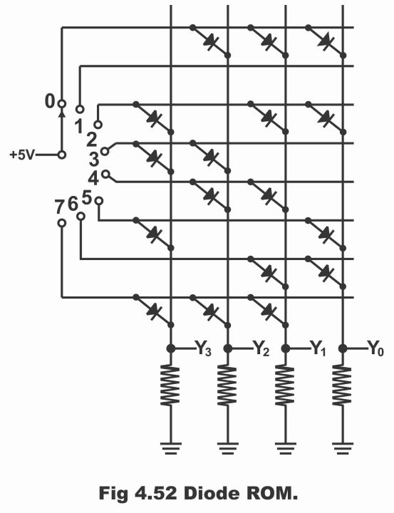
When switch is on position 0 (address 0) current passes through the line above diode (i.e. all diodes on top or 0 line become forward biased as a result of being connected to +5V or they tend to operate as a closed switch). As 3 diodes have been fixed on this line, therefore output linked with these diodes becomes high or 1. Whereas all other outputs besides this particular one, remain low or zero. In such a situation, ROM’s output is as under:
Y3 Y2 Y1 Y0 = 0111
When rotary switch is brought to position 1, the second line activates (i.e. this line connects with +5V and diodes mounted on this line, start to conduct). As a result, following output is received:
Y3 Y2 Y1 Y0 = 1000
Similarly, when we connect rotary switch with rest of the positions or addresses, we get output according to the nibbles present in the table (Y0 – Y3)
As ROM diodes are constructed according to the data given in an integrated circuit, therefore these diodes designed within an IC chip, can neither be replaced nor can they be detached (i.e. diodes are fixed within an IC or tailored permanently). Therefore, data can be read only by means of providing voltages on different memory locations. This is the reason a ROM is known as a read–only memory.
For further explanation, a diode ROM circuit has been illustrated in figure 4.53 (a) which performs the function of translating decimal to gray code (i.e. this diode ROM is programmed with gray code). Gray code has been illustrated in figure 4.54 along with equivalent decimal numbers and equivalent binary numbers.
If rotary switch is rotated and brought on position 6 (as has been illustrated vide figure a), in such a situation, value of ROM outputs (A, B, C and D) is 0101 or LHLH (remember that each position of a rotary switch is linked with an address). If the given diagram is studied carefully, it becomes evident that by spinning the rotary switch to decimal position 6, no diode exists on two outputs B and D of a total of four outputs existing on the line. These outputs are connected with ground through resistors due to which both these outputs (B and D) become zero or low. However inversely, diodes having been mounted with the other two outputs on line number 6 (i.e. A and C), turn forward biased by means of receiving +5V. Resultantly, outputs A and C become 1 or high. Thus, following gray output is obtained by means of bringing rotary switch on position 6. The same has been illustrated in the table as well.
A B C D = 0101
Figure (a) – output indicator gray code
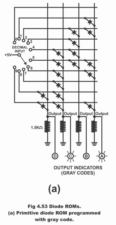
Figure (b) – output indicators gray code
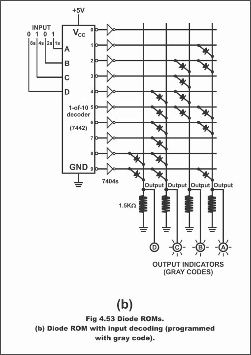
Figure 4.53 – Diode ROMs (a) – primitive diode ROM programmed with gray code (b). diode ROM with input decoding (programmed with gray code)
Figure 4.54 Gray Code
| Decimal Number | Binary Number | Gray Code Number |
| 0 | 0000 | 0000 |
| 1 | 0001 | 0001 |
| 2 | 0010 | 0011 |
| 3 | 0011 | 0010 |
| 4 | 0100 | 0110 |
| 5 | 0101 | 0111 |
| 6 | 0110 | 0101 |
| 7 | 0111 | 0100 |
| 8 | 1000 | 1100 |
| 9 | 1001 | 1101 |
| 10 | 1010 | 1111 |
| 11 | 1011 | 1110 |
| 12 | 1100 | 1010 |
| 13 | 1101 | 1011 |
| 14 | 1110 | 1001 |
| 15 | 1111 | 1000 |
Similarly, every rotary switch position, provides output in gray code form through a diode ROM. In figure (b) a better type of a diode ROM has been illustrated, wherein a decoding chip has been installed instead of resorting to a primitive rotary switch technique for selection of the addresses. In the beginning of this circuit, a one – of – 10 decoders (which converts binary to decimal) has been used (i.e. 7442 TTL IC), which decodes just one out of 10 decimal outputs at a given period of time (i.e. only one of its 10 output lines at a time remains in a low activated state). Inverters have been fixed on the output side of this decoder which converts low decoder output to a high output. Thus, inverter performs a job of selection of the corresponding row.
For example, if binary input is 0101 (i.e. decimal 5) as has been depicted in figure (b). Under such a situation, 7442 decoder’s output 5, will be activated on a low state (i.e. it will be low). This low output is transmitted on to inverter (mounted behind the decoder), which converts it into a high output. It needs to be remembered here that at that time all other outputs are low as compared to 5. This high output forward biases three diodes (which have been connected to A, B and C outputs) mounted on line 5. Resultantly, A, B and C outputs become high, whereas output remains low. As a result, following output is received.
ABCD = 0111 = LHHH
It has also got to be remembered that this resultant output is an equivalent grey code of binary input 0101, as has been demonstrated via the table. Similarly, equivalent gray codes can be determined by dint of changing addresses and binary input values of IC’s.
Commercially Available ROMs
We know that apart from being a high-density and non–volatile memory device, ROM is a permanent storage device, on which reprogramming is not possible. At present, roughly more than 500 different ROMs are available.
A number of corporations and manufacturers fabricates commercial ROMs. They range from a small bipolar TTL unit to a very large-capacity CMOS or NMOS ROMs. Normally, commercial ROMs are often available in the form of DIP (dual in- line package). Some of the ROMs available in market are as under:
TT – 7488 … 256 bits organized as 32 x 8
TTL – 74187 … 1024 bits organized as 256 x 4
TTL 74S370 … 2048 bits organized as 512 x 4
CMOS TMS47C512 … 524, 288 bits organized as 65536 x 8
7488 TTL ROM can store up to 32 words, of which every word consists of 8 – bits. Thus, its overall capacity is 256 bits. A TTL 74187 ROM can store up to 256 words, each word of which has 4 bits. Thus, its total capacity is 1024 bits. TTL 74S370 unit or ROM can store a total of 2048 bits, which are configured as 4 – bits with 512 words. The larger capacity TMS 47C512 ROM can store up to 524, 288 bits. There are overall 65536 words having been arranged in 8 – bits. This type of ROM can transmit can transmit or process such a large number of words just in 200 to 350 nano seconds or it can access such a large number of words in just 200 to 350 nano seconds. This type of ROMs is normally used in personal computers.
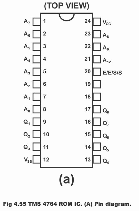
In figure 4.55, pin diagram (along with functions of different pins) of a Texas Instruments designed commercial TMS 4764 ROM has been illustrated. It contains a total of 8192 words, each word of which consists on 8 – bits. This ROM is encased in a 24 – pins DIP (i.e. it has a total of 24 pins and it is in the DIP shape). The chart in figure (b), indicates nomenclatures and functions of these pins. In this IC, overall 13 input lines (A0 to A13) or address inputs are present in order to address 8192 (i.e. 213) memory locations, in which A0 is LSB (Least Significant Bit) and A12 MSB (Most Significant Bit) of the word address. The access time of TMS-4764 ROM keeps changing within a range of 150 to 250 nano seconds. However, it depends on the version of purchased chip. Permanently stored data can be accessed on output via pin Q1 to Q8. Here Q1 pin is LSB whereas Q8 pin is MSB. Output pins (Q1 – Q8) are enabled by means of pin 20. Pin 20 can be programmed by the manufacturer in case it is active low or active high.
Figure 4.55 – TMS 4764 ROM IC (A). Pin diagram (b). Pin nomenclatures incorporated
Applications of ROMs
Read-only memories (ROMS) are used in order to store data and programs on a permanent ground. Moreover, these are also commonly used in computer system programs, look–up tables, decoders, and as character generators. Besides, ROMs are also used for the solution of combinational logic problems.
Previous Topic: BCD Encoder circuit diagram and truth table in digital electronics
Next Topic: Flip-Flop Combinational logic circuits and Sequential logic circuits
For electronics and programming-related projects visit my YouTube channel.
Discover more from Electronic Clinic
Subscribe to get the latest posts sent to your email.