Digital to Analogue D/A converter in Digital Electronics
Last Updated on March 23, 2023 by Engr. Shahzada Fahad
Table of Contents
Digital to Analogue (D/A) Conversion
The process of converting numerous digital input signals to equivalent analogue output signals or voltage is called digital to analogue (D/A) conversion. D/A converter is a fundamental part of multiple systems. In order to understand D/A, it is essential that we must have a full knowledge about the necessary components or elements e.g. operational amplifiers and binary weighted inputs etc. being used in it, the detail of which is as follows;
The operational Amplifier
It is necessary to have some knowledge about an operational amplifier prior to understanding the process of a digital to analogue converter (DAC), because these devices also have basic importance in analogue to digital converters apart from DACs.
An operational amplifier which is shortly known as op–amp, is a device which consists of two inputs (i.e. inverting and non-inverting) and one output. Its input impedance is extremely high whereas its output impedance is very low. Moreover, its voltage gain is also inordinately high (which can also be set with an external resistor). The symbol of an op – amp has been represented in figure 10.4 (a), wherein inverting and non- inverting inputs are clearly visible. Inverting input has been reflected via a negative (-) sign whereas non – inverting input by a positive (+) sign. An output is also visible towards the right of this symbol. When an operational amplifier is used as an inverting amplifier, an input resistance (Rin) and a feedback resistance (Rf) is mounted alongside it in order to set its voltage gain (Remember that it is never being used alone), as has been illustrated by the diagram. Feedback resistance Rf and input resistance Rin control voltage gain according to the following formula;
AV (Voltage gain) = Rf/ Rin = Vout / Vin
Here, the negative sign indicates phase inversion, which means that when this amplifier is being used as an inverting amplifier, its output signal is completely inverted to its input signal from its shape viewpoint. That’s if input voltage is positive, output voltages are negative.
Figure 10.4 – The operational amplifier (op – amp)
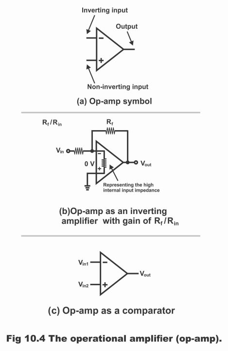
Suppose that the values of both resistors Rin and Rf used along an operational amplifier are 10KΩ (i.e. Rin = 10KΩ and Rf = 10KΩ). In such a situation, the voltage gain is as follows;
AV = Rf /Rin = 10,000/ 10, 000 = 1
If the value of input voltage (Vin) is 5V and output voltage (Vout) also 5V, then voltage gain can also be determined by means of voltage instead of resistor as follows;
AV = Vout / Vin = 5/5 = 1
Here, Vout/ Vin means close loop gain (feedback means transmitting some part of output back to input through Rf). Remember, the open loop voltage gain of this amplifier is even higher than approx.100,000.
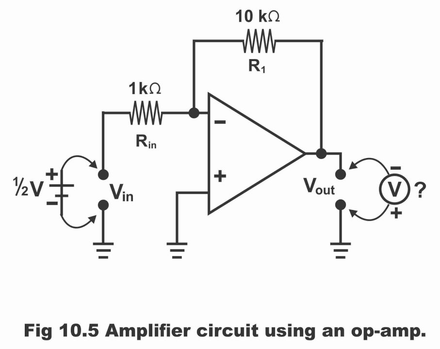
Now presume that values of input and feedback have been changed to 1KΩ and 10KΩ respectively, as has been illustrated in the diagram. In such a situation, voltage gain of the circuit will be as follows;
AV = Rf /Rin = 10, 000/ 1000 = 10
If the input voltage value of amplifier is +0.5V (or ½V) then in such a situation, voltages on output under, will be as follows;
AV = Vout / Vin
10 = Vout / 0.5 or Vout = 10 x 0.5 = -5V
It has become clear from afore – mentioned detail that how can gain of an operational amplifier be changed by means of changing the mutual ratio of input and feedback resistors. Thus, an operational amplifier is an important component of any D/A converter, which is used as a summing amplifier in a converter and amplifier gain can easily be set through input and feedback ratio.
Figure 10.5 – Amplifier circuit using an Op – Amp
According to the configuration of inverting amplifier as illustrated in figure 10.4 (b), inverting input of the operational amplifier is on ground potential (approx. 0V), because differential voltage existing between both inputs are very low due to feedback and extremely high loop gain (approx. higher than 100,000). As non – inverting input has been grounded, therefore inverting input is on about 0V, which is known as a virtual ground.
In other words, when an operational amplifier is used as an inverting amplifier, its non – inverting input (input with + sign) is grounded, whereas signal voltages are provided on inverting input (input with – sign), as has been illustrated vide diagram (b). As the voltage gain of an operational amplifier is pretty high, therefore very low (usually in micro volts) voltage are provided on its inverting input, which are considered as approx. 0 volt according to initial estimates and input impedance of the inverting input is considered almost infinity. As such, owing to both these factors, inverting input of an operational amplifier turns into a virtual ground point (i.e. point with zero voltage and zero current). Remember that basic difference between an ordinary ground and a virtual ground is that an ordinary ground consists of zero voltage and can sink any quantity of current (i.e. any quantity of current can transmit through it).
When operational amplifier is used as a comparator, as has been illustrated in the figure 10.4 ©, two voltages are provided on its inputs. When a very minute difference emerges between these input voltages, then amplifier makes a comparison between them, due to which it sets on any one of its two saturated states (i.e. high or low). However, this process depends on voltages of which one of the inputs are high.
Binary-Weighted-Input D/A Converter
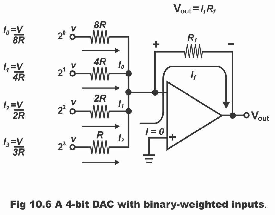
In one of the methods of D/A conversion, such type of binary weighted resistor divider network is used, the resistance values of which reflect binary weights of digital codes’ input bits. In figure 10.6, this type of a 4 – bit digital to analogue converter (DAC) has been illustrated. According to the figure, current either flows through every input resistor shown in the figure or does not flow at all. This depends on the level of input voltage. If the value of input voltage is low or 0 (i.e. binary 0), in such a situation current’s value will also be 0. If the value of input voltage is high (i.e. binary 1), currents’ value will also be 1. The quantity of current flowing through an input resistor depends on the value of that input resistor. As input values of each input resistors are different, therefore a different current pass through each of the resistors. This has been illustrated in the figure.
Figure 10.6 – A 4-bit DAC with binary – weighted inputs
Suppose that we again want to convert binary obtained from the digital processing unit to analogue value of 0 – 3V output. In order to understand operation of any decoder, first of all its truth table is drawn, which reflects all its possible situations. In figure 10.8, truth table of a D/A converter consisting of four inputs (A, B, C and D) has been illustrated. As these inputs are in binary form, therefore it is no so important to know about the precise value of these inputs. Here, every binary is equivalent to about 0V and every logic 1 or binary 1 equal to about +3V to +5V. Analogue output voltages received from decoder’s output have been reflected in the rightmost column of the table. According to the table, when binary 0000 appears on D/A converter or decoder’s input, its output is 0V. When input is 0001 (as shown via line 2 of the table) in such a situation, output is 0.2V. Similarly, when decoders’ input binary is 0010, its output becomes 0.4V (as has been indicated vide line number 3 of the table). It becomes evident from a careful observation of the table that as we keep moving from line 4 to line 16, an increase of 0.2V is witnessed in analogue output voltage after every row.
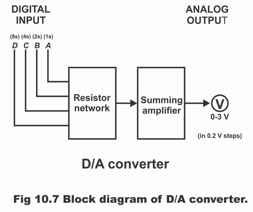
Figure 10.8 – Truth Table for D/A Converter
| Digital Inputs | Analogue Output | ||||||
| Rows | D | C | B | A | Volts | ||
| Row 1 | 0 | 0 | 0 | 0 | 0 | ||
| Row 2 | 0 | 0 | 0 | 1 | 0.2 | ||
| Row 3 | 0 | 0 | 1 | 0 | 0.4 | ||
| Row 4 | 0 | 0 | 1 | 1 | 0.6 | ||
| Row 5 | 0 | 1 | 0 | 0 | 0.8 | ||
| Row 6 | 0 | 1 | 0 | 1 | 1.0 | ||
| Row 7 | 0 | 1 | 1 | 0 | 1.2 | ||
| Row 8 | 1 | 1 | 1 | 1 | 1.4 | ||
| Row 9 | 1 | 0 | 0 | 0 | 1.6 | ||
| Row 10 | 1 | 0 | 0 | 1 | 1.8 | ||
| Row 11 | 1 | 0 | 1 | 0 | 2.0 | ||
| Row 12 | 1 | 0 | 1 | 1 | 2.2 | ||
| Row 13 | 1 | 1 | 0 | 0 | 2.4 | ||
| Row 14 | 1 | 1 | 0 | 1 | 2.6 | ||
| Row 15 | 1 | 1 | 1 | 0 | 2.8 | ||
| Row 16 | 1 | 1 | 1 | 1 | 3.0 | ||
The point worth noting about resistor network illustrated in the figure 10.7 is that existence of 1 on input B implies that its value is twice the value of 1 present on input A. Similarly, value of 1 on input C is four times the value of 1 on point A (i.e. double the value of 1 on input B).
For this purpose, in order to maintain value of every next digital input doubled as compared to the value of previous input, various resistor configurations are used (i.e. resistors can be used in network form through multiple configuration). For example, resistor divider network, which has previously been discussed or binary ladder network etc. Remember that binary ladder is such a resistive network, output voltages of which are appropriately weighted according to the sum of digital inputs, whereas in resistive network, direct real translation occurs from a digital signal to an analogue voltage. However, in a digital to analogue converter, either one of the resistive divider networks or a ladder can be used.
The summing amplifier illustrated in diagram 10.7 receives output voltage from resistor’s network and amplifies it up to the correct quantities of analogue output voltages given on the right most column of table illustrated via figure 10.8. The summing amplifier is normally available in a specific IC unit form, which is called operational amplifier (op – amp).
Thus, a D/A converter or a specific type decoder consists of two parts i.e. a group of resistors (which is either a ladder resistive network or resistive divider network) and an operational amplifier (which operates as a summing amplifier)
Binary Ladder or R/2R Ladder D/A Converter
Binary ladder is another method being used for digital to analogue conversion (and it is also known as R/2R ladder) which consists of such resistive networks, output voltages of which are proportionate to the binary weight of the digital inputs provided on it. Remember that a ladder network consists of resistors having two values only.
In figure 10.9, a R/R2 ladder type DAC has been illustrated consisting of 4 bits. As it has resistors consisting of just two values (i.e. R and 2R), therefore all issues or drawbacks existing on binary weighted DAC are eliminated or removed completely. However, it must be remembered that either one of any these two (i.e. resistive divider network or R/R2 ladder network) can be used.
Figure 10.9 – An R/2R ladder DAC
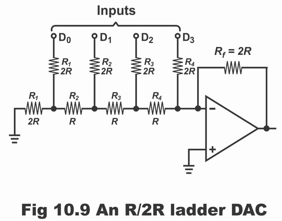
In order to understand the operation of a R/2R ladder DAC, first assume that D3 input is high (+5V) and rest of the inputs (D0, D1, D2) are on ground level (0V) or low. This condition provided on converter represents binary number 1000. As D0, D1, D3 resistances of the circuit are low, therefore value of resistance equivalent to this circuit (RFQ = equivalent resistance) is 2R, which has been shown through figure 10.10 (a). As a result of the inverting input being on virtual ground level, no current passes through this 2R equivalent resistance and circuit’s entire current (I = 5V/2R) transmits on Rf via R7. Thus, output voltage -5V are received, which is evident from diagram (a). Remember that inverting input (-) of the operational amplifier is always retained equal to almost 0 owing to a negative feedback. Therefore, entire current instead of passing through inverting input, passes via R1.
Figure 10.10 – Analysis of R/2R ladder DAC
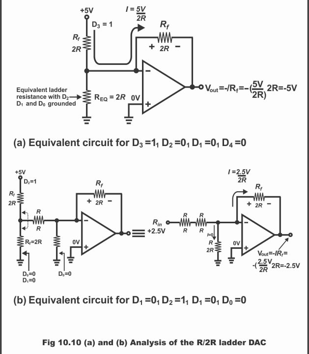
When D2 input is high or +5V and rest of the inputs are on ground levels, this condition applying on the converter represents binary 0100. The equivalent circuit formed under this situation has been illustrated in figure (b). According to Thyonian theorem, if we look behind R8 (i.e. solve this circuit according to Thyonian theorem), we receive +2.5V on R, which is RTH (which are Thyonian voltage VTH), series. As a result of these voltages, current I (I = 2.5V /2R) passes from Rf, owing to which -2.5V are received from output, as has been illustrated via figure (b). It is worth remembering here that no current passes towards ground from operational amplifiers’ inverting input and equivalent resistance. This is because 0V exists parallel to them as a result of virtual ground.
When D1 input is on +5V and rest of the inputs are grounded, as has been illustrated via figure (c), it represents 0010 state. Looking inwards from R8, when this circuit is solved according to Thyonian theorem, we get +1.25V in R series, as has been elaborated via an equivalent circuit shown in figure (c). As a result of these voltages, current I (I = 1.25V+2R) passes through R1, due to which -1.25V output voltages are received.
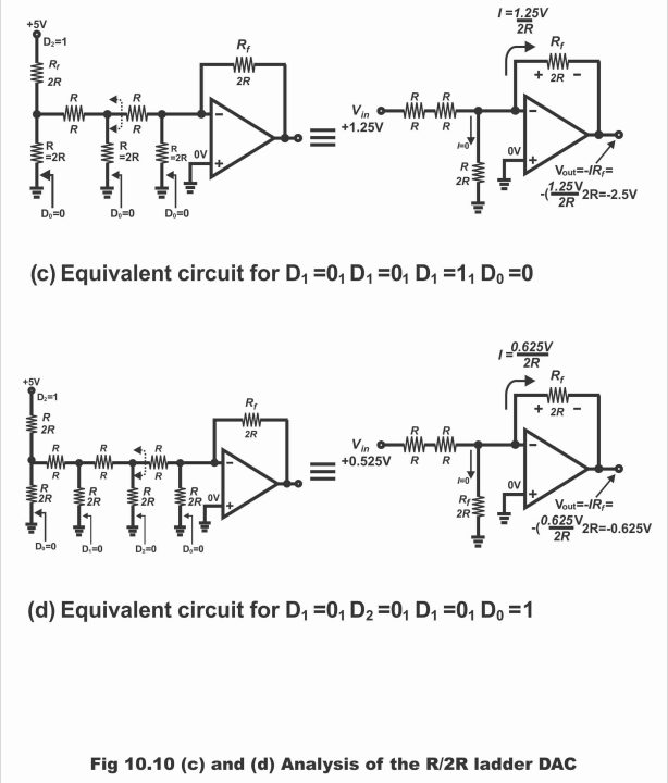
Similarly, when input D0 is high or +5V and rest of the inputs are grounded, then converter’s input status reflects 0001, as has been illustrated vide figure (d). Looking back from R8, when Thyonian resistance and Thyonian voltages of this circuit are determined with the help of Thyonian theorem, we get their values as R and 0.625V respectively. As a result of these voltages, I current transmits through R1 (i.e. I =0.625/2R), thus -0.625V are received.
It is clear from the afore – mentioned detail that every next downward coming low weighted input produces half voltages as compared to its upward lying input. Which proves that output voltages are proportionate to binary weight of input bits.
A Basic D/A Converter
In figure 10.11, a simple digital to analogue (D/A) converter circuit has been displayed, which comprises two sections. The left section of this circuit is called resistor network which consists of R1, R2, R3 and R4 resistors, whereas on the right section of this circuit, a summing amplifier is set, which consists of a feedback resistor Rf (10KΩ) and two supplies (+10V and -10V). The value of input voltage (Vin) of this circuit is 3V, which are transmitted on A, B, C and D switches, whereas measurement of output voltage (Vout) is carried out by means of a volt meter set on circuit’s output. The operational mechanism of this converter circuit is as follows;
When all switches are open or on ground level (0V), 0V exists on amplifier’s input bit A, as a result 0V are also received on output. This state has been reflected by line number 1 of the truth table in figure 10.8.
Figure 10.11 – A D/A converter circuit
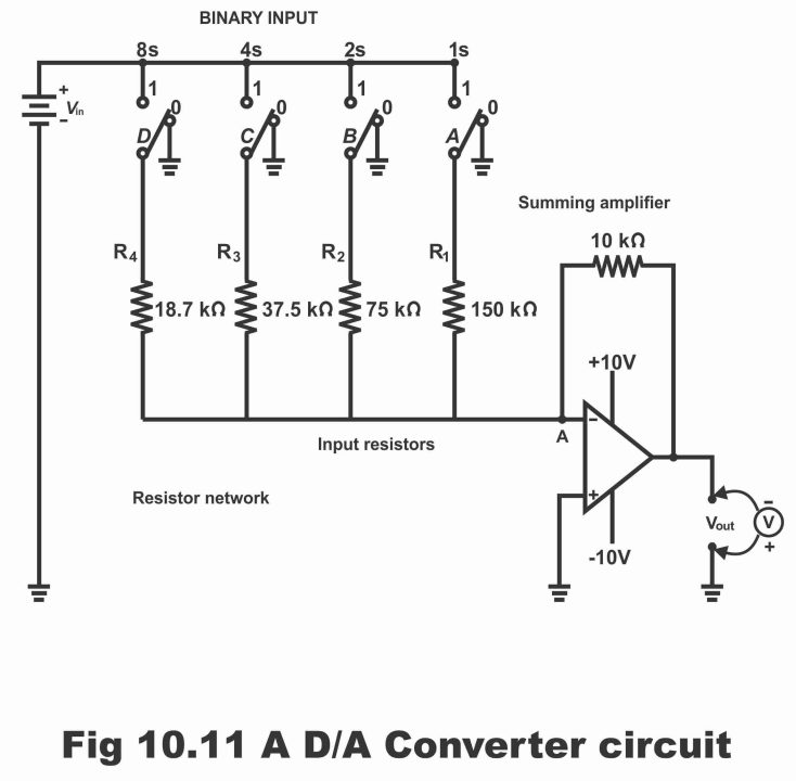
Now suppose that switch A has been set on logic 1 position (i.e. switch A has been closed while remaining three switches are open or on logic 0 position). In such a situation, 3 volts are received on operational amplifiers input. As amplifier’s gain depends on its feedback resistor Rf (which has a value 10KΩ) and input resistor Rin (which has been denoted here by R1 and its value is 150KΩ), therefore its value is as follows;
AV = Rf/Rin = 10,000/150,000 = 0.066
In order to find output voltage (Vout), this gain is always multiplied by input voltage as follows, (because we know that AV = Vout / Vin).
Vout = AV x Vin = 0.066 x 3 = 0.2V
Thus, when only switch A remains closed and all remaining switches are open, or when input is binary 0001, in such a condition, the value of output voltage is 0.2V, as has been illustrated vide row number 2 of the table.
Now if binary 0010 is applied on D/A converter, or only switch B is set on logic 1 position (i.e. switch B remains closed while remaining three switches remain open), in such a situation 3V are received on operational amplifier and its gain is as follows;
AV = Rf / Rin = 10,000/ 75,000 = 0.133
When this gain is multiplied by input voltage, output voltage value is received as 0.4V, as has been illustrated vide line number 3 of the table i.e.
Vout = Av x Vin = 0.133×3 = 0.4V
Similarly, now if switch D is closed only whereas all other switches are kept opened (i.e. binary 1000 is applied on converter) the values of amplifier’s gain and output voltage values are as follows;
AV = Rf /Rin = 10,000/18,700= 0.535
Vout = AV x Vin = 0.535×3 = 1.6V
This value of output voltage reflects row number 9 of the table. If we cautiously study this table (which has been depicting 16 possible conditions of a 4-bit binary digit) it becomes obvious that an addition of 0.2V occurs in output voltage of D/A converter after every binary count. Its basic reason is that resistances of resistor network keep declining from right to left, therefore values of voltage being received on output, tend to increase.
When all of the switches are activated i.e. when switches are closed or set on logic 1 state, operational amplifier’s gain increases up to 1. As a result, exact 3V are received from its output. This has been indicated by the last line of the table. Therefore, multiple binary bits are provided on summing amplifier by means of opening or closing different switches alternately. This reflects output in an analogue form by means of summing these different amplifiers’ bits combinations. Remember that remaining within limits of an operational amplifier’s power supply (10V), any input voltage can be provided on its converter. And the number of binary digits can be increased by means of raising the number of switches. However, the number of resistors also increases by doing so, as a result of which circuit’s overall accuracy is adversely affected.
Ladder Type Digital to Analogue (D/A) Converter
This type of digital to analogue converter consists of a ladder resistor network (that’s why it is called ladder type digital to analogue converter) and a summing amplifier. In figure 10.12, a similar D/A converter circuit has been illustrated, where in a ladder resistor network (which is also known as R/2R resistor network) has been used. This resistor network provides appropriate weighting for binary inputs. The advantage of this type of configuration is that resistors with only two values are used into it. The value of every horizontal resistors R1, R2, R3, R4 and R5 having been used in this figure is 20KΩ whereas the value of every perpendicular resistor R6, R7, R8 and Rf resistor is 10KΩ. As resistors of just two values (10KΩ and 20KΩ) have been used in the circuit and as values of all horizontal resistors except Rf mounted on the ladder is twice as compared to the value of vertical resistors, therefore the converter where in a ladder network has been used, is known as R/2R resistor network. Remember that summing up amplifier set on a ladder type D/A converter circuit also functions like a resistor network D/A converter circuit (which has already been discussed above) and it is also being provided a dual power supply (i.e. -10V and +10V). Moreover, operational mechanism of this circuit is also analogous to the operation of afore – mentioned basic D/A converter circuit.
Figure 10. 12
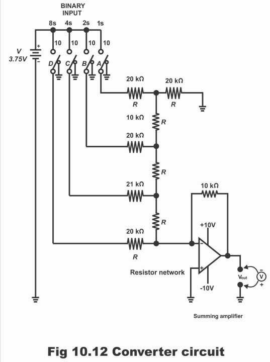
Figure 10.13 – Truth Table for D/A Converter
| Binary Inputs | Analogue Output | ||||
| 8s | 4s | 2s | 1s | Analogue Output | |
| D | C | B | A | Volts | |
| 0 | 0 | 0 | 0 | 0 | |
| 0 | 0 | 0 | 1 | 0.25 | |
| 0 | 0 | 1 | 0 | 0.50 | |
| 0 | 0 | 1 | 1 | 0.75 | |
| 0 | 1 | 0 | 0 | 1.00 | |
| 0 | 1 | 0 | 1 | 1.25 | |
| 0 | 1 | 1 | 0 | 1.50 | |
| 0 | 1 | 1 | 1 | 1.75 | |
| 1 | 0 | 0 | 0 | 2.00 | |
| 1 | 0 | 0 | 1 | 2.25 | |
| 1 | 0 | 1 | 0 | 2.50 | |
| 1 | 0 | 1 | 1 | 2.75 | |
| 1 | 1 | 0 | 0 | 3.00 | |
| 1 | 1 | 0 | 1 | 3.25 | |
| 1 | 1 | 1 | 0 | 3.50 | |
| 1 | 1 | 1 | 1 | 3.75 | |
When only switch 1 is activated or brought on logic position 1, i.e. binary 0001 is applied on converter (remember that binary 0 means 0V and here binary 1 means 0.75V) in such a situation, following analogue output voltage are received from converter’s output;
Vout = 3.75 x 20 + 0 x 21 + 0 x 22 + 0 x23/ 24 – 1
= 3.75 +0 + 0 +0/16 -1 = 3.75/ 15 = 0.25V
Now if binary 0010 is applied on D/A converter’s input (i.e. only switch B of the four switches is closed or on logic 1), following analogue output voltage are received from converter’s output;
Vout = 0 x 20 + 3.75 x 21 + 0 x 22+ 0 x 23/ 24 – 1
0 + 7.50 + 0 + 0/15 = 7.50 / 15 = 0.50V
Similarly, now if switch D is closed, whereas rest of the switches are open (i.e. binary 1000 is applied on converter) following output is obtained from D/A converter;
Vout = 0 x 20 + 0 x 21 + 0 x 22+ 3.75 x 23/ 24 – 1
= 0 + 0 + 0 + 3.75 x 8/ 16 – 1
= 30/15
= 2.00V
Remember that this formula can also be used in a basic digital to analogue converter consisting of resistive network, by means of which analogue voltage’s value can be obtained directly without ascertaining amplifier gain.
The operation of a ladder type D/A converter has been illustrated with detail through a table in figure 10.3. it must be remembered here that 3.75 input voltage are being used on this circuit instead of 3V and as a result of every binary count, an increase of 0.25V occurs in analogue output (which has been reflected in the right most column of the table). It should also be remembered that the presence of every zero on the input side means that 0 volts have been provided on this input. Whereas the presence of 1 on every input of table means that 3.75V have been provided on this input. As output of commonly used TTL counters and other ICs is very close to 3.75V’s input voltage, therefore 3.75V value input voltage have been used here. Thus, given inputs (A, B, C, D) in the diagram, set directly with output of any TTL – IC can be made to operate according to the table given in figure 10.13. The number of binary digits or number of binary places on a D/A converter shown in the diagram can also be increased as required (i.e. 16s, 32s and 64s etc.). Thus, heart of a D/A converter consists of resistor network and summing amplifier, by means of which binary words of any value can easily be converted to equivalent analogue words.
Previous Topic: Digital to Analogue & Analogue to Digital Converters
Next Topic: Analogue to Digital Conversion in Digital Electronics
Discover more from Electronic Clinic
Subscribe to get the latest posts sent to your email.

