Half Wave and Full Wave Rectifier With Equation Examples
Last Updated on March 29, 2022 by Engr. Shahzada Fahad
Table of Contents
Diode As A Rectifier
A diode is a device, which is used for converting AC to pulsating DC. It is structured from a PN junction which is composed of silicon or germanium crystal. We know that when some PN junction is forward biased, it conducts (i.e. it passes current inside it) and when it is reverse biased, it practically has no conduction (i.e. it does not allow current to pass through it). In other words, it completely blocks current in the event of reverse bias. Thus, due to this attribute of PN junction or diode, (that it allows only one-way flow of current), it is mostly applied as a rectifier in power supplies. A rectifier is actually a circuit, in which AC is converted to pulsating DC through applying one or more diodes. Rectifiers are available in the following two forms:
- Half Wave Rectifier
- Full Wave Rectifier
Half Wave Rectifier
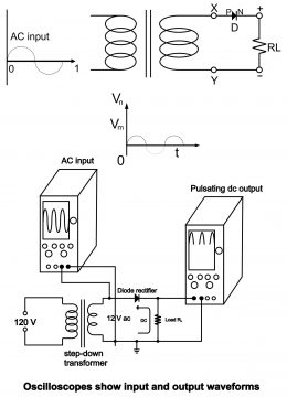
The process of converting AC to pulsating DC output is called rectification. A rectifier, which converts only half cycle (or only positive half) of an input AC to pulsating DC, is called half wave rectifier. In fig 1, circuit or diagram of a half wave rectifier, with input and output waves has been displayed.
Construction
In the displayed circuit, the transformer’s output has been connected with a diode and a loader resistor. Both diode and loader resistor are inter-connected in a series. AC voltages have been supplied on transformers input, which continuously changes polarity in relation to applied voltage’s frequency. The semiconductor diode, applied in the circuit, provides rectified voltage to load resistor R1.
Working Method
During the positive half cycle of AC input voltage, the upper point (X) of transformer’s secondary is positive compared to the lower point (Y), therefore, the diode will be forward bias (ON). In this way diode will conduct, and forward current will pass through the load resistor (R1) (i.e. the flow of conventional current will begin the moment the diode conducts). Due to this current, output voltage parallel to the load (value of which depends on the values of current and load resistor i.e. V=IR) will emerge.
During the negative half cycle (when input voltages are negative in the second half of the cycle), the higher point of transformer’s secondary winding (point X) is negative compared to its lower point (Y), due to which diode becomes reverse biased (or off). Therefore, no current will pass between diode and load during the negative half cycle, due to the inability of diodes to conduct. Thus, no voltages will appear parallel to R1.(that’s the value of voltage parallel to load resistor will be zero). Remember, that maximum reverse voltages are received parallel to diode, during the negative half cycle.
As half wave rectifier provides AC input parallels to load voltage on negative half cycle and prevents negative half cycle from moving towards the load, therefore pure DC voltages do not generate on half wave rectification, rather they are pulsating. i.e. such output DCs voltages also have a component of AC, which is known as a ripple. In other words, half wave rectifiers, do not have a steady DC, rather output is in the form of a pulsating DC wave, the ripple frequency of which equals ripple voltage frequency. This wave can be seen parallel to R1 through an oscilloscope. (figure 1). A filter circuit is used in order to get rid of ripples or achieve a steady-state output. Following results are obtained through this process of rectification.
Average Values
The value depicted via a DC meter, is called its average value.
(i). Vdc=Vin/π=0.138Vin
or
Vdc=1/2π ∫π⁰?⍬=1/2π ∫π⁰ (Vm Sin⍬) d⍬
=Vm/2π = Vm/2π [+1-(-1)]
=Vm/π=0.318Vm
(ii). Idc= Vdc/RL=Vm/πRL=0.318Vm/RL=0318Iπ
(iii). Irms=Im/2=051m
Peak Inverse Voltage
The maximum voltage found in a reverse direction parallel to a diode is called peak inverse voltage. Under the present situation, its value normally is V in:
Form factor=rms value/average value=0.5Im/0.318Im=1.57
Efficiency
The ratio between output DC power and overall AC input provided by the circuit is called efficiency i.e.
η= Pout /P in
Where P out= I2dc RL
Pin= I2rms (rd+RL)
Here RL means load resistance and rd means AC resistance of diode
η= I2dc RL/I2rms (rd +RL) x 100…(1)
By entering the values of Idc and Irms in equation (1) (because Idc=0.381 and Irms=0.51)
η= (0.3181m) 2. RL/ (0.51m) 2 (rd+RL) x100
=0.101124 I2m. RL/0.25 I2m(rd+RL)x100
=0.101124 I2m. RL/ 0.25 I2mrd+ 0.25 I2mRL … (2)
Taking RL I2m 0.251 common from divider of equation (2)
=0.0.101124 I2m . RL/0.25 I2m RL (rd/RL +1) x100
=0.406/rd/RL+1 x100= 40.6/I+rd/RL percent
Ignoring diode resistance rd
η=40.6% ………………………(3)
Ripple Factor
We know that a diode‘s (or DC power supply’s) output consists of a pulsating DC instead of steady DC voltage. Its reason is presence of some AC components in output DC. Such AC components are called ripples. Compared to DC voltage, through quantity of ripples or measurement of variations in AC voltage, one can understand about the purity of DC power output. It is called the ripple factor (γ). Thus, the ripple factor of a single phase half wave rectifier is 1.21. The formula of ripple factor is as below:
γ= √(Form Factor) 2-1
Remember that in a half way rectifier circuit, ripple frequency equals supply frequency (i.e. ripple frequency is same as supplied on input). In such circuits, the ripple factor is greater than the rectification factor and it is used in places, where less current and more voltage is required.
Following supply voltage received from load resistor from above-mentioned equations
Vdc= Vm/π-Idc rd
Here Vm/π reflects the average quantity of voltage on secondary terminals and Idc rd denotes DC voltage drop on the diode.
Full Wave Rectifier
As the name suggests, it is a rectifier circuit, which supplies output to a full cycle input AC voltage (or both positive and negative parts of a cycle), in the form of a pulsating DC. Following two circuits are applied for full wave rectification in case of array of diodes type of transformers.
(A). Full Wave Centre-Tapped Rectifier Circuit
(B). Full Wave Bridge Rectifier Circuit
Full Wave Centre Tapped Rectifier
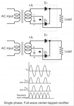
In this full-wave rectification method, a center-tapped transformer, the secondary of which is center-tapped (due to which secondary winding divides into two parts) and two diodes are used. Which function or conduct turn by turn after each half cycle? A full-wave center-tapped rectifier circuit, consisting a center-tapped transformer and two diodes, has been illustrated in figure 2
Working Method
After providing signals to transformer’s primary winding on AC input, when secondary winding’s point A gets more positive in relation to end B within positive half cycle, D1 turns forward bias and D2 reverse biased. Through D1 conduction, current passing through the load via D1 reaches the transformer’s center tap. Remember that during the positive half cycle; D2 being reversed biased cannot conduct. Therefore, conventional current transmits only via D1 load and the higher part of the secondary winding.
During a negative half cycle, the upper part of the secondary winding (A) is negative compared to the lower-end (B) (In other words, the lower end of the secondary winding is positive while the upper end is negative). Therefore, lower diode D2 conducts due to being forward biased, whereas upper diode D1, does not conduct due to being reverse biased. In such a situation, conventional current flows in the lower part of D2 load and secondary winding.
From the above discussion, it is evident that irrespective of input voltages’ polarity, one of the two diodes always remain forward biased, which passes current endlessly through the load. Further, as the direction of current drifting via load during both half cycles of AC voltages, always remain the same, therefore, DC voltages always ensue on output (or parallel to load resister)
Following outcomes are elicited via such rectification.
Average Values
(i) Vdc= 2Vm/π=0.636Vm (twice the HW rectifier value)
i.e. in this method, a two times average value is received compared to a half way rectifier.
(ii) Idc = 2 Im/π= 0.636Im
(iii). Irms= 0.707Im
(iv). Form factor= Irms/Iav= 0.707Im/0.636Im
Peak Inverse Voltage (P.I.V)
The peak inverse voltage rating of every diode under this method of full wave rectification is 2Vm
Efficiency
Efficiency of a full wave rectifier is doubled (i.e. 81.2 percent) compared to a half way rectifier, owing to the fact that both halves of AC input supply are operated under full wave rectification, while in a half wave rectification, only one cycle is used. Thus,
η=Pout/Pin=I2dcRL/I2rms(rd+RL)
Substituting and simplifying, we get
η=81.2%/I+rd/RL=81.2%… if rd=0
Ripple Factor
Ripple factor on a half way rectifier is pretty small compared to a full wave rectifier (i.e. 0.482). With respect to the form factor, value of a ripple factor can be determined as follows.
γ= F2-12
Full Wave Bridge Rectifier
This circuit is most widely used in electronic DC power supplies. In this circuit, 4 diodes and a transformer are used, the secondary winding of which is not center-tapped. As 4 diodes are connected just like a wheat stone bridge, therefore, it is known as a bridge rectifier. A single-phase full wave bridge rectifier has been illustrated in figure 3.
Working Method
During first half of input AC cycle, when the upper end or point A of transformer’s secondary winding is positive compared to the lower end or point of winding, diode D1 and D3are forward-biased Thus, conventional current completes its cycle via D1 load and D3. Remember, that when diodes D1 and D3 are forward biased, diodes D2 and D4 are reversed bias at that moment. Therefore, during the first half or positive half cycle, D2 and D4 do not conduct (i.e. no flow of current occurs)

When input cycle is negative, or when the polarity of points A and B mutually changes during the second half of input AC cycle, diodes D2 and D4become forward bias while diodes D1 and D3 turn reverse biased (i.e. remain off). Thus, through conduction of D1 and D2, unidirectional flow of current via load becomes achievable. Therefore, the direction of flow of current through load remains the same during both half cycles. Thus, full wave DC output generates due to the conduction process of two diodes in turns.
Note: Almost the same results from a full-wave bridge rectifier circuit are achieved as from a full-wave center-tapped rectifier circuit.
Alternative Explanation of Full-Wave Bridge Rectifier
This circuit is most widely used in electronics DC power supplies.
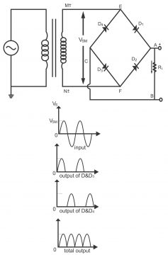
In such circuits, there are 4 diodes (instead of 2) and a transformer, which is not center-tapped. As a complete secondary winding of the transformer is applied in such a circuit, therefore, double voltages (maximum voltages Vm) are achieved from this circuit compared to double diode center-tapped circuits. A full-wave bridge rectifier circuit along with its input and output waves, has been illustrated in figure 4
Working
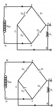
During the positive half cycle of input AC supply, the secondary terminal of transformer M becomes positive and terminal N negative (as indicated via figure 5 “a”). In such a situation, diodes D1 and D2 get forward biased (ON), while diodes D2 and D4 become reverse biased (OFF). Therefore, current transmits through route MEABCFN, due to which voltage drop occurs parallel to load resistor, R1.
During negative half cycle of input AC supply, secondary terminal N becomes positive while M becomes negative (as AC regularly modifies its polarity during everyhalf cycle) shown in figure (b). Under such conditions, diodes D2 and D4are forward biased while D1 and D3 reverse biased. Therefore, flow of current within circuit occurs on the conduit NFABCEM. If the direction ofcurrents’ flow through RL in above both situations is examined, we come to know that during both AC input half cycles, direction of flow of current within resistance RL remains same (i.e. during positive and negative cycles of supply, the direction of flow of current through RL always remains from A towards B). Thus, points A of bridge rectifier always works as an anode whereas point C as a cathode. Output voltage accrued parallel to RL, has been shown in figure 4. The frequency of in-voltage is twice as higher compared to supply voltage.
Average Values
Average values of a full-wave bridge rectifier are equal to the values accruing from full a wave center-tapped rectifier (which have been discussed in the previous pages) i.e.
(i). V dc= 0636 Vm
(ii). I dc= 0.636 Im
(iii). Irms= 0.707 Im
(iv). Form factor= 1.11
Peak Inverse Voltage
The PIV rating of each of the four diodes used in a full-wave bridge rectifier, is Vm, while in the case of an ordinary full-wave rectifier, the rating of every diode equals 2Vm (which can easily be understood with the assistance of figure 6). Remember, this diagram only represents a condition, wherein the bridge is provided a positive half cycle of supply. In such a situation, D2 and D4 are open (off) due to reverse bias. If the flow of current occurs on path MEACFN, then total voltage, due to secondary voltage and D1 and D3 conduction, equals total of drop voltage parallel to RL. This total is equal to 2Vm=Vm+Vm

Ripple Factor
Its value equals a common full wave rectifier’s value.
γ= 0.482
Efficiency
Its value also equals a common full wave rectifiers’ value i.e.
η= 81.2% … (ignoring diode’s resistance)
Advantages
Due to small cost, tiny size and being trustworthy, bridge circuit is more admired than center-tapped transformer rectifier. Some advantages of bridge rectifier are as under:
- There is no need of a center-tapped transformer
- Requires a very small size transformer
- Occupies a very small space
- It is also less heavy
- It is cheap from price point of view
- More lasting and trustworthy
- More effective in high voltages
- The peak inverse rating of every diode is low
There is just one disadvantage of this method, i.e. it uses 4 diodes instead of 2
Comparison between HW & FW rectifiers
Full-wave rectifiers, whether a center-tapped transformer type or bridge type, is preferred over half-wave rectifiers due to the following reasons:
- Double DC voltages accrue parallel to load i.e. HW= Vdc. Fw=2xVdc
- Has low ripple factor
- Has greater rectification efficiency
- The PIV rating of diodes applied in a bridge rectifier equals the PIV rating of an HW rectifier. However, the PIV rating of diodes of an FW rectifier with respect to a center-tapped transformer is twice the rating of diodes in an HW or bridge rectifier.
- The aforementioned 3 advantages are also achieved through the application of an FW rectifier composed of a center-tapped transformer against Half Wave rectifier.
- Center-tapped transformer FW rectifiers are preferred over bridge rectifiers in low voltages, in case maximum output voltage parallel to RL is just 0.7 volt less in case of practical silicon diodes and the PIV rating of diodes is not good. The maximum output voltage, which the FW bridge rectifier provides a parallel to RL, is lesser than the value of voltage drops of two diodes (1.4 volts). And it is considered a great drawback in low-dc-voltage applications. However, PIV ratings assume great importance (due to the costs factor) in the case of applications requiring high dc voltages and the voltage drop of both diodes (i.e. 1.4 volts) becomes insignificant. Therefore, the FW rectifier is preferred for supplying high dc voltages parallel to load.
For electronics and programming-related projects visit my YouTube channel.
Previous article: PN junction and Next article: different types of Junction methods
Discover more from Electronic Clinic
Subscribe to get the latest posts sent to your email.
