Different Types of Junction Methods in Electronics
Last Updated on March 29, 2022 by Engr. Shahzada Fahad
Table of Contents
Description:
Different types of junction methods- in this article, we will discuss different types of junction methods in very detail Grown Method, the Alloy method, Diffused Junction method, Epitaxial Growth junction method, Point Contact Junction method, Drift Field Junction method, Surface Barrier Junction method, Re-crystallized Junction method.
Semiconductor Diode Fabrication
The electrical properties of a semiconductor diode depend on the following two factors.
- Applied Material
- Applied type of junction (PN)
Germanium (Ge) and Silicon (Si) are the most extensively used materials as semiconductor diodes. As germanium has high electrical conduction as compared to silicon, therefore, it is enormously used in low and medium-powered diodes. On the contrary, silicon can be operated at a high temperature compared to germanium, therefore, silicon is considered suitable for high-powered applications. Gallium arsenide (GaAs) is a new material, which has useful characteristics of silicon and germanium, thus application of this new material has rapidly been increasing. PN junction can be produced through any one of the following junction methods
- Grown Junction method
- Alloy Junction method
- Diffused Junction method
- Epitaxial Growth junction method
- Point Contact Junction method
- Drift Field Junction method
- Surface Barrier Junction method
- Re-crystallized Junction method
A brief detail of the above-mentioned chemical methods has been given below:
Grown Junction Method
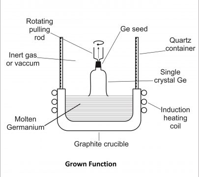
This is the oldest and most popular method being used for the construction of a diode. In this method, a pure intrinsic semiconductor and a P-type impurity are provided heat to such an extent (placing it in a quartz crucible for production of a PN junction) that both matters meltdown and get dissolved in each other. A small semiconductor crystal called seed is placed in this melted solution. Then seed crystal is rotated in solution at a pace that melted matter sticks to this seed. It is then pulled out. Melted material that sticks with crystal seed becomes hard after having cooled down. Now material stuck with the seed crystal has the same characteristics, as which seed has. If only P-type impurity has been pooled in solution, the grown crystal will be a P-type semiconductor. However, if the seed crystal is doped with N and P-type impurity one by one, it means that N and P-type layers are being produced on a semi crystal. This generated crystal is then cut and converted into small PN junctions.
In other words, according to the method of grown junction for constructing diodes, a crystal seed of desired impurity level is sunk in the melted semiconductor matter. This melted semiconductor material is kept in a crucible made of graphite (as shown in figure 1). Then, this crystal is pushed out from melted semiconductor material slowly through a rod or shaft. Remember, that shaft has also to be rotated during this process. When the crystal is being pulled out through the material, P and N-type impurities are added turn by turn in order to produce a PN junction. Then this large-sized crystal is cut into several small-sized diodes. Remember, the area of the grown junction diode is adequately large for passing or handling high currents (due to which its power rating is also high)
Alloy Junction Method
This method of construction of a PN junction is a very simple and easy one.
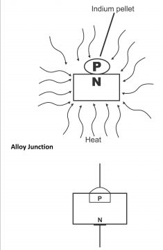
Junction diodes produced through the alloying process are capable of high peak inverse voltage ratings and high current ratings. And its junction capacitance is also greater due to a large junction area. In this method, a small indium dot or pellet or dot/pellet of any other type of impurity is placed on the surface of an N-type silicon wafer, both are heated up at a temperature higher than the melting point of indium(about 150 degrees centigrade) (as illustrated in the figure 2. As a result, indium melts, and some portion of it absorbs into silicon (base material). Then the temperature is lowered, due to which silicon freeze again and assumes the shape of a single crystal based on the PN junction (as illustrated through diagram b)
In other words, a P-type impurity is put on an N-type substrate or N-type semiconductor crystal (i.e. a small dot or pellet of indium is placed) and both are heated up to a melting point, due to which both materials combine together and convert to an alloy (i.e. indium pellet and N-type semiconductor material heated up to such a limit, that pellet, having melted, enters into semiconductor material and as such special identity of this pellet abolish altogether after going into the semiconductor, as illustrated by the diagram. As indium is a trivalent impurity, therefore, the place where these two substances combine becomes P-type material). When both are chilled, a PN junction pops up on one end of substrate alloy (i.e. both materials assuming crystal shape, emerge as PN conductor)
Diffused Junction Method
This method of PN construction is most broadly used and well-liked. This method of production of semiconductor junction diodes is also relatively cheaper and can be controlled more accurately. However, this method is more time-consuming as compared to the alloy process. The diffusion process is used in solid or gaseous shapes. In this method, particles of high concentration region are drifted or diffused towards surrounding particles of low concentration regions. The basic distinction between the alloy process and diffusion process is that there is no liquefaction process in the method of the diffused junction. Heat is only used just to increase the activity of concerning substances.
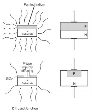
In this method of PN junction, a thin section of N or P-type semiconductor (called a wafer) is combined with any impurity which is in a gaseous or vaporized state. This process is conducted at a very high temperature, in which impurity element vapors enter penetrate into the wafer (or they get diffused). A thin mask or veil is first put on N-type semiconductor crystal, then the mask and crystal are exposed to vaporized gaseous impurity. There is an open space in the middle of the mask, where gaseous impurity collides with crystal. Thus, impurity atoms spread across (diffuse) N-type crystal, and a P-type semiconductor matter is, thus produced. Resultantly, a PN junction is achieved.
Solid Diffusion
In the solid diffusion process, a P-type impurity (e.g. Indium) is painted above an N-type substrate and both are heated. Until this impurity forms a P-type layer via absorbing or diffusing at some distance in the substrate.
Gaseous Diffusion
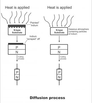
In this method, an N-type material is heated up inside a chamber (which consists high concentration vapor of an acceptor impurity) as illustrated by figure (b). Thus, N-type impurity, absorbing or diffusing in the substrate, constructs semiconductor diodes’ or PN junctions’ P-type layer. During the diffusion process, the size of the P region is controlled by exposing only one part of N-type material (while the rest of the portion is covered through coating or putting on a thin layer of SiO2). Metal contacts are put for fixing leads on the surface of every region. Remember, that the role of N and P-type materials are mutually interchangeable. This method is mostly used in the manufacturing of semiconductor diodes.
Epitaxial Junction Method
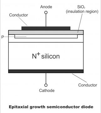
The word epitaxial has been derived from two Greek words “epi” meaning upon and “taxis” meaning arrangement. Thus, epitaxial means the arrangement of one thing above another. Such types of junctions are manufactured on an N-type wafer placed in the high-temperature chamber. The base wafer of an N-type material is linked with a metal conductor (figure 4). This N-type material is excessively doped for mitigating resistance characteristics. After which, applying the diffusion process, a P-type layer is put upon it. Through the application of diffusion technique in P type silicon conductor, anode metal conductor is also fixed according to the shape. In this method, the operation of junction production takes place atom to atom or in a balanced manner and it is crystal shaped. The biggest advantage of such junctions is that they have minimum resistance.
Point Contact Junction Method
This N-type wafer is composed of germanium or silicon (its area is about 1.25 square millimeters and thickness 0.5 millimeters), the front part of which has been soldered with base metal through radio frequency heating (figure 5), and the second part of which, Phosphor Bronze (tungsten) or spring (also called cat’s whiskers) has been placed through pressing. Junction is manufactured by passing a very high current through spring wire or N-type substrate. While crystal face along with wire point is kept positive. Thus, the resulting heat pushes away some of the atom electrons found in the small region around the point of contact. Thus, holes develop as a result of the emission of electrons. This small N-type material region converts into P-type material region as illustrated in figure
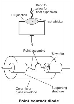
In other words, a point-contact semiconductor diode is manufactured by penetrating a phosphor bronze spring or whisker into an N-type substrate. After which, a very high current is passed through whisker and substrate for a very brief time, due to which atoms, passing through wires, penetrate into N-type material. Thus, a P region comes into being in the wafer.
The junction capacitance of the PN junction, due to its small area, is very low (normally 1 pekoe farad or less). Therefore, point contact diodes are mostly used in places where large frequencies exist e.g. microwave mixers or detectors, etc. The disadvantage of the junction’s low area results in its low current ratings and compared to junction type diodes, less commendable characteristics can be anticipated from such type of diode.
Drift Field Junction Method
This method of PN junction manufacturing closely resembles the method of alloy method. In this method, some area is diffused, while other portion remains undiffused, due to which the flow of current gets faster. However, capacitor charging time is quite less in this method.
Surface Barrier Junction Method
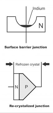
In this method, doping material is arranged inside a small inbuilt on the upper part of P or N-type material. This material combines with some part of semiconductor material by means of heating it to an apposite temperature as shown in figure 6. Thus, the thickness of the base material gets less.
Re-Crystallized Junction Method
In this method of junction manufacturing, layers of P and N-type materials are recombined in such a manner, that one of the layers gets more heat, while other end of the layer is kept chilled. Resultantly, material at one end mixes due to melting/ liquefaction. It happens so long as heat exists. However, as heat is removed, both ends cool down, material shrinks and assume the shape of a crystal shown in figure 6.
Diode Ratings or Specifications
Normally, manufacturers provide ratings or datasheets of semiconductor devices in two segments. One of the segments contains a thorough detail about the particular device, while a comprehensive examination of the device is furnished through graphs and applications in the second segment.
It is very necessary to understand the specifications and have detailed knowledge about any particular use of a diode, which is given in the datasheet, provided by the manufacturer of the device. These details include diodes’ absolute ratings, specific operating conditions, mechanical data, and graphs prepared from curves depicting its various functions. Sometimes, additional data is also provided depending on the type of diode, which normally contains details about frequency range, switching time, thermal resistance level, etc.
Remember, absolute maximum ratings refer to a maximum value of current and voltage, which can be supplied without the device getting damaged or useless. The ratings of a device cannot be ignored for obtaining a better and more reliable output. Some important specifications of diodes are as follows.
Peak Inverse Voltage or PIV
These are the maximum reverse voltages that are provided without any damage to the diode. In other words, the maximum voltage that a diode can sustain without developing a defect or becoming useless is called peak inverse voltage. It is also known as peak reverse voltage (PRV), reverse breakdown voltage (VRB or VR), or maximum reverse voltage (VRM).
Average Forward Current
It is a continuous forward current, which a diode can transmit at normal temperature (25⁰C), or a continuous forward current passing through a diode at normal temperature, which is called its average forward current. It is denoted by IF (av). Average forward current is also called maximum steady-state forward current (IF or IF. Max) or repetitive forward (current, which a diode can safely pass or handle)
Forward Surge Current
A surge current can be defined as a large current, which a diode can safely handle for a very short period of time (i.e. one second). In other words, a large current passing safely through a diode for a very brief period of time is called a forward surge current (IFS).
Maximum Forward Voltage
The maximum forward voltage which a diode can put up with without being burnout is called maximum forward voltage, denoted by VFM
Forward Voltage
These are voltages that at a certain temperature pass a certain value of forwarding current through a diode. It is denoted by VF
Reverse Current
It is a maximum reverse saturation current at a given temperature and maximum reverse voltage. Normal reverse current is denoted as IR and its maximum value as IRM
Power Dissipation
It is the maximum power, which a diode can safely emit or consume in the air at a normal temperature (25⁰C)
Reverse Recovery Time
The maximum time required for bringing a device from on to off condition is called the reverse recovery time of the device. It is denoted by trr and its value is usually measured in nanoseconds (ns).
Remember, that the forward voltage drop value in a diode, should not exceed 1 volt, while the maximum current value should be 1-200mA.
Breakdown Voltage
High reverse voltages on which PN junction breakdowns due to a sudden increase in reverse current are called breakdown voltages.
Knee Voltage
Forward voltages, on which current passing through the junction, increase very rapidly, is called knee voltages. In the case of germanium, its value is 0.3 volt, and in silicon, it is 0.7 volt.
For electronics and programming-related projects visit my YouTube channel.
Previous article: half-wave and full-wave Rectifier and Next article: Filters Circuit and Need of Filters
Discover more from Electronic Clinic
Subscribe to get the latest posts sent to your email.


Thanks for best work you’re doing
Hi Mr. Shahazada Fahad. I am Jaimin Trivedi-Research Scholar from Navrachana University, Vadodara. I am doing Phd and i have a query regarding the images shown in this page for P-N junction methods like grown and diffusion methods. Could you provide me your mail id so that we can communicate and discuss it further?. Kindly reply me at the earliest.