Logic Gates in Digital Electronics Complete Guide
Last Updated on February 5, 2022 by Engr. Shahzada Fahad
Table of Contents
Logic Gates and Digital Electronics Introduction:
Digital electronics, digital technology or digital (electronic) circuits are electronics that operate on digital signals. Digital electronic circuits are usually made from large assemblies of logic gates (often printed on integrated circuits), simple electronic representations of Boolean logic functions.
The main elements which play a vital role in Digital Electronics are given below:
- Logic Gates
- Adders
- Subtractor
- Comparator
- Flip Flops
- Timers and Clocks
- Shift Register
- Counters
- Memories
- Multiplexer or Data Selector
- Demultiplexer or Distributor
- Encoder
- Decoder
- Code Converter
In this article, we will only learn about Logic Gates.
Learn how to use Logic Gates in PLC Ladder Logic Programming.
Logic Gates:
In digital electronics, the decision making capability of the gate circuit is called logic, and a type of logic circuit that performs a specific logical operation e.g AND or OR etc is called a gate. So, the logic gates are the type of electronic circuits that makes logical decisions, and their output depends on the preset rules. The logic gates can have multiple inputs but always has a single output. A gate is just like a switch which can be ON or OFF. The ON state represents logic 1, while the OFF state represents logic 0. A gate can not only add, subtract, count, etc but can also store the information. The most common types of the gates are
- AND
- OR
- NAND
- NOR
- NOT
- XOR
- XNOR
So, a logic gate is the building block of a digital system. The gates are also called logic circuits, digital circuits, and switching circuits. The logic gates are used in different IC families, for example, TTL “Transistor-Transistor Logic”, ECL “Emitter-coupled Logic”, MOS “Metal Oxide Semiconductor”, and CMOS “Complementary Metal Oxide Semiconductor”.
Positive and Negative Logic:
The digits 0 and 1 are very important in computing systems, which represents any of the two possible states of an electronic circuit or a device. It really doesn’t make any difference if you call these two states
- ON and OFF
- Closed and Open
- High and Low
- Plus and Minus
- True and False
- Up and Down
In positive logic, the digit 1 represents
- ON circuit
- A closed switch
- High voltage
- A true statement
- Up
While in a negative logic the digit 0 represents
- OFF circuit
- An open switch
- Low voltage
- A false statement
- Down
So, the positive and negative logic can be defined as
If in a digital or computing system the OFF circuit or open switch or low voltage is represented by the binary digit 0 and the ON circuit or closed switch or high voltage is represented by the binary digit 1 this is called Positive Logic. While on the other hand, if in a digital or computing system the OFF circuit, open switch, or low voltage is represented by the binary digit 1 and the ON circuit or closed switch or high voltage is represented by the binary digit 0, this is called negative logic.
Let me explain this with the help of an example. Let’s consider a digital system consists of two voltage levels 0V and 5V. Let’s say 1 represents 5V and 0 represents 0V. In such a case a positive logic system is created, while on the other hand if 1 represents 0V and 0 represents 5V, in such a case a negative logic system is created. This can be clearly explained with the help of a simple circuit given below.
As you can see in the circuit diagram, a lamp is connected between the two terminals A and B. The terminal B is also connected with the earth. This lamp is connected with the 5V battery through a switch “S”, when the switch is open then with respect to the earth 0 Voltsare available on terminal A, so, the lamp remains OFF. When we close the switch, then with respect to the earth 5 Volts are available on terminal A, so the lamp will turn ON. So this is how we get the two possible output states (0V and 5V) with respect to the earth or terminal B. One more thing that I would like to add, before I am going to explain the types of Logic Gates.
In some cases, the digit 0 and digit 1 can be represented by two different values. For example, in an electronic circuit, there are two voltage levels 2V and 10V. In a situation like this 10 volts can be represented by the digit 1 and 2 volts can be represented by the digit 0. The same thing applies to negative voltage levels, let’s say
-2V and -8V
1 = -2V
0 = -8V
As -2V > -8V
Types of Logic Gates:
OR Gate:
OR Gate is the physical realization of the logical addition. The operation is represented by (+).
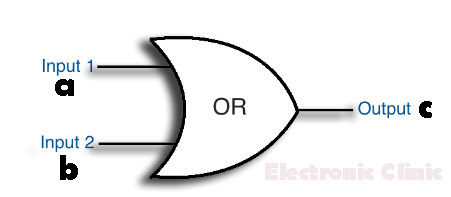
OR Gate is an electronic circuit that generates an output signal of 1 if any of the input signals is 1 and generates an output signal of 0 if all the inputs are 0. The OR Gate can have multiple inputs but, it has a single output. The graphic symbol of the OR Gate is given below.
OR Gate Logic Symbol:
Using two inputs a and b and the output is c.
The algebraic function of the OR Gate is
c = a + b
OR Gate Truth Table:
This is quite clear from the OR Gate truth table. On the right side, you can see the output is 0 when both the inputs are 0. While the output is 1 when any of the input signals is 1 or High.
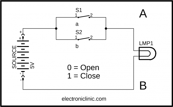
The switching circuit for the OR Gate is given below.
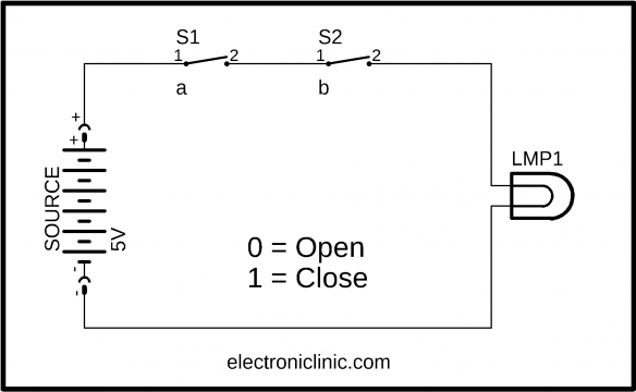
The switches S1 and S2 are considered as 1 when they are closed, while the open positions of the switches S1 and S2 are considered as 0. The Lamp will glow only if any of the inputs a or b are closed, or both the switches are closed. The Lamp will not glow if both the switches are open.
Diode OR Gate:
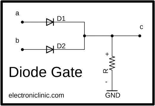
Let’s dig deeper to understand the function of the OR Gate. Let’s replace the two switches S1 and S2 with diodes D1 and D2, this makes the Diode OR Gate, as you can see in the circuit below.
Two diodes D1 and D2 are connected in parallel with the output c. The working principle of such a Diode Gate circuit is as follows.
- When 5 Volts are applied at the input a, the diode D1 becomes forward bias and start conducting due to which the current flows through the resistor R, and 5 Volts are dropped across the resistor R. Due to which 5 volts will be available at the output c. In other words, If the input a is High and input b is Low. In a situation like this, the upper diode D1 will conduct “ON” and the lower diode D2 will not conduct “OFF”. As the diode 1 is ON so will get 5 Volts across the resistor R. In a practical circuit, if we include the diode voltage drop then at the output the available voltage will be around +4.3 Volts.
- When 5 Volts are applied at the input b, the diode D2 becomes forward bias and start conducting due to which the current flows through the resistor R, and 5 Volts are dropped across the resistor R. Due to which 5 volts will be available at the output c.
- If 5 volts are available on both the inputs, as the diodes are connected in parallel, so still we get +5 volts on the output c.
- If no voltage is applied, both the diodes remain in off state i.e. not conducting, so on the output, we will get low voltage.
Transistor OR Gate:
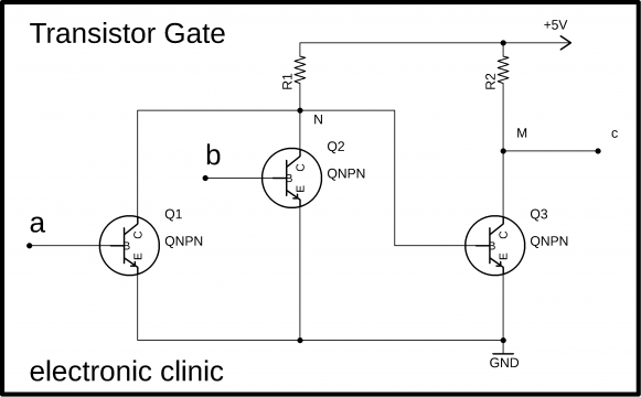
A transistor OR Gate circuit as you can see above consists of 3 NPN type transistors Q1, Q2, and Q3. The collectors of the transistors Q2 and Q3 are connected with the 5 volts power supply through resistors R1 and R2 respectively. These are the pull-up resistors. The emitters of all three transistors are connected to the ground.
In this transistor OR Gate circuit, the two inputs are represented by a and b, while the single output is represented by c. Let’s discuss the working principle of the transistor OR Gate.
High = +5 volts
- When the input a is high the transistor Q1 is turned ON i.e. the transistor Q1 saturates and the emitter of the transistor Q1 shorts with the collector. As you can see in the circuit diagram, the collector of Q1 is also connected with the collector of Q2 and point N, and is also connected with the base of the transistor Q3. So as the emitter of Q1 is short with the collector, this way the ground which is connected with the emitter becomes available at the collector of Q1 and Q2 and also become available at the base of Q3 this turns OFF the transistor Q3, so at the output c we get +5 volts, and at the point N we get 0 volts.
- If input a is low and input b is high. In a situation like this only the transistor Q2 will turn ON i.e. the transistor Q2 saturates, due to which ground will be available at point N, as you can see the point N which is the collector of Q2 is also connected with the base of the transistor Q3. So ground will be available on the base of Q3 as well, due to this the transistor Q3 is cut off i.e. the transistor Q3 remains OFF. So +5V will be available at the output c.
- If both the inputs a and b are high, the ground will be available at the base of transistor Q3 which of course turns OFF the transistor Q3, so +5V becomes available at the output c.
- If both the inputs are low. The transistor Q1 does not conduct and remains OFF or Open, so it feels like if the transistor Q1 is not even present in the circuit. The transistor Q2 also remains in the cut off state, but as you see the collector of the transistor Q2 is connected with the +5V through the resistor R1 so this pulls the collector of Q2 transistor to +5V, due to which +5V becomes available at point, which is given to the base of the transistor Q3 and the transistor Q3 is turned ON i.e. the transistor Q3 saturates and this way the emitter of the transistor Q3 is short with the collector. So 0 Volts or ground becomes available at the output c.
AND Gate / AND Operator:
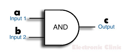
AND Gate is the physical realization of the logical multiplication. The operation is represented by ( . or ^ ). AND Gate is an electronic circuit that generates an output signal of 1 only if all the input signals are 1. The graphical symbol for AND Gate is given below. Using two inputs a and b, and the output is C. The graphic symbol of the OR Gate is given below.
AND Gate Logic Symbol:
Using two inputs a and b and the output is c.
The algebraic function of the OR Gate is
c = a . b
AND Gate Truth Table:
This is quite clear from the AND Gate truth table. On the right side you can see the output is 0 when any of the inputs is 0. While the output is 1, when all the inputs are HIGH.
The switching circuit for the AND Gate is given below.
The switches S1 and S2 are considered as 1 when they are closed, while the open positions of the switches S1 and S2 are considered as 0. The Lamp will glow only, if both the inputs a and b are closed. The Lamp will not glow if any of the switches S1 and S2 are open.
Diode AND Gate:
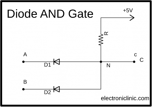
A diode AND Gate circuit is shown above. The circuit consists of the Pull-Up resistor R connected with a 5V power supply, and two diodes D1 and D2. The diodes are connected in the reverse biased configuration. Let’s discuss the working principle of the diode AND Gate.
- When both the inputs A and B are low. Both the diodes are forward biased and conduct. Due to which 5 volts drop across the resistor R and at the input C we get 0 volts or ground.
- If the input A is high and input B is low. In a situation like this the diode A is reversed biased, which becomes completely open, and behaves like as if it is not even in the circuit. While on the other hand the diode D2 is forward biased due to which the +5V drops across the resistor R and at the output C we get 0 Volts or ground.
- If the input A is low and input B is high. In a situation like this, the diode A is forward biased, due to which the 5 volts drop across the resistor R and at the output C we get 0 volts or ground, while the diode D2 remains open.
- If both the inputs A and B are high. In a situation like this both the diodes are reversed biased i.e. open, which offers high resistance, due to which +5V will be available at the output C.
Transistor AND Gate:
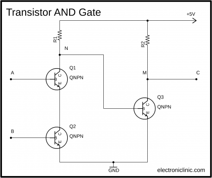
The transistor AND Gate is shown above. The circuit consists of 3 NPN transistors Q1, Q2, and Q3, and two Pull-Up resistors R1 and R2. The circuit is connected with a +5V power supply. The two inputs are represented by A and B, while the output is represented by C. The emitters of both the transistors Q2 and Q3 are connected with the ground, while the emitter of Q1 is connected with the collector of the transistor Q2. A wire from the collector of Q1 represented by the point N is connected with the base of transistor Q3. Let’s discuss the working principle of the Transistor AND Gate circuit.
- When both the inputs are low, this way the point N is pulled to +5 Volts. This means at point N we have 5 volts. As you can see the point N is connected with the base of transistor Q3, so the transistor Q3 is turned ON i.e. the transistor Q3 saturates, the emitter gets short with the collector and this way 0 volts will be available on the output C.
- If any of the two inputs A and B is OFF, the circuit behaves in the same way as discussed above. So at the output C we get 0 volts or ground.
- If both the inputs are high i.e. both the transistors Q1 and Q2 saturates, which acts as the wire this way ground will be available at point N, which is connected with the base of the transistor Q3. This turns OFF the transistor, which acts as the open circuit and offers high resistance due to which +5 volts will become available at output C.
NOT Gate:
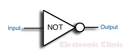
NOT Gate is the physical realization of the complementation operation. NOT gate is an electronic circuit that generates an o/p signal which is the reverse of the input signal. NOT gate is also known as inverter, because it inverts the input signal, that is if the input is 1 then the output will be 0, when the input is 0 the output will be 1. The NOT Gate has only 1 input and a single output. The graphic symbol for the NOT Gate / inverter is given below.
NOT Gate Logic Symbol:
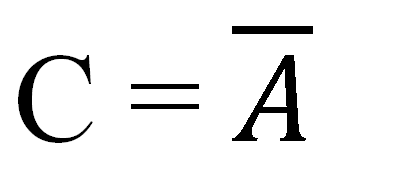
The Algebraic function of the NOT Gate is given as
NOT Gate Truth Table:
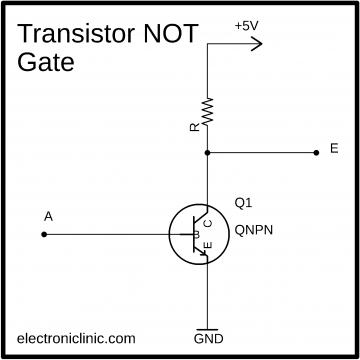
Transistor NOT Gate:
The transistor NOT Gate is shown above. To implement a transistor NOT Gate you only need a few electronic components like resistors and a transistor. You might be thinking why I said “resistors”, while there is only one resistor in the circuit diagram above.
In reality, when we use such circuits we also add a resistor with the base of the transistor, as there are bipolar junction transistors. A practical circuit will look like this,
You can use this circuit with different types of sensors to signal the controller board like for example Arduino, or any other 5V compatible controller board. Let’s discuss the working principle of the Transistor NOT Gate.
- If the input A is high, the transistor turns ON i.e. the transistor saturates so 0V will be available on the output E.
- If the input A is low, the transistor is turned OFF i.e. the transistor is cut off, due to which it offers the maximum resistance and point E is pulled to +5V. so this way for the high input we get low output and for the low input, we get high output.
NOR Gate:
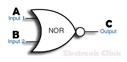
NOR Gate is the complement of the OR Gate. NOR Gate is an electronic circuit that generates an output signal of 1 if both the inputs are 0 and generate an output signal of 0 if any of the input signals is 1. The graphic symbol for the NOR Gate is given as.
NOR Gate Logic Symbol:
The two inputs are represented by A and B, while the output is represented by C.
The Algebraic function of the NOR Gate is given as
NOR Gate Truth Table:
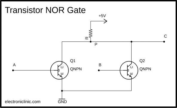
Transistor NOR Gate:
The Transistor NOR Gate is shown above. The collectors are connected together and also the emitters of both the transistors are connected together. The +5V power supply ground is connected with both the emitters. While the +5V are connected with the collectors through a resistor R. Let’s discuss the working principle of the Transistor NOR Gate Circuit.
- When both the inputs A and B are low i.e. both the transistors are cut-off, due to which these offer maximum resistance so at the output C +5V will be available.
- If the input A is high and input B is low. As input B is low, so this transistor will not conduct and acts as the open circuit, which feels as if the transistor is not even present. While the input A is high so this transistor will conduct i.e. this transistor saturates, so at the point, P 0V will be available, which becomes available at the output C.
- The same above mechanism applies to when the input A is low and input B is high. We will get 0V at the output.
- If both the inputs A and B are high i.e. both the transistors saturates so at the output 0V will be available.
NAND Gate:
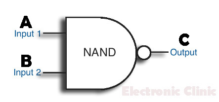
NAND Gate is the complement of AND Gate. NAND Gate is an electronic circuit that generates an output signal of 1 that is the o/p of NAND Gate will be 1 if any of the i/p is zero and will be zero if all the inputs are 1. The graphic Symbol for the NAND Gate is given below using two inputs A and B and the output is C.
NAND Gate Logic Symbol:
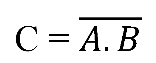
The Algebraic function of the NAND Gate is given as
NAND Gate Truth Table:
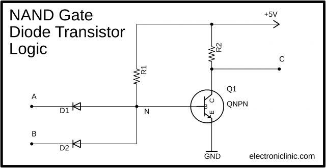
NAND Gate using Diode-Transistor Logic “DTL”:
Let’s see how this circuit works.
- If both the inputs A and B are low, as you see both the diodes D1 and D2 are connected in the reverse-biased configuration. So both the diodes will conduct. Due to which 0V will be available at point N. This will turn OFF the transistor Q, which becomes open and offers high resistance. So at the output, we get +5V or 1.
- If the input A is high and input B is low. When the input A is given 1 or 5V the diode D1 will be reversed biased and becomes open, and feels like if the diode D1 is not even present in the circuit. As 0V is available at the input B, so the diode D2 is forward biased, due to which 0V will be available at point N, this turns OFF the transistor Q i.e. transistor is cut off due to which it offers maximum resistance and as a result, +5 volts are available at the output C.
- If both the inputs A and B are high, in a situation like this both the diodes D1 and D2 are reversed biased i.e. both the diodes act as an open switch. The point N is pulled to +5V, which turns ON the transistor i.e. the transistor Q saturates, this connects the output C with the ground. So at the output, C 0V will be available.
Exclusive OR Gate / XOR Gate:
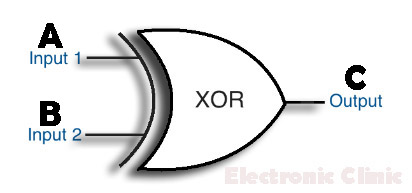
Its abbreviation is X-OR Gate. Its symbol is similar to the symbol of OR Gate with the addition of one curved line before the OR Gate. The exclusive OR Gate with two inputs is shown below.
Exclusive OR Gate / XOR Gate logic symbol:
The Algebraic function or Boolean expression is given as
A XOR B = C
Or
C = A ⊕ B.
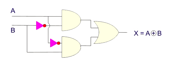
The exclusive OR Gate is not the basic logic gates. It can be obtained by using two NOT gates, two AND gates, and one OR Gate.
Exclusive OR Gate / XOR Gate Truth Table:
From the exclusive OR Gate truth table, we can see that for the dissimilar input the output is High, while for the same inputs the output is low.
Exclusive NOR Gate:
This gate is the complement of the X-OR gate. So the output of this gate is the complement of the output of X-OR Gate. It is abbreviated as X-NOR Gate.
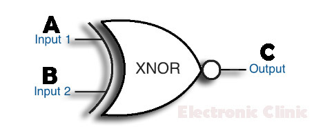
Logically it is equivalent to an exclusive OR Gate followed by an inverter. The exclusive NOR Gate with two inputs is shown below.
Exclusive NOR Gate Logical Symbol:
The Algebraic equation or the Boolean expression of the exclusive NOR logic Gates is given as,
Exclusive NOR Gate / XNOR Gate Truth Table:
In the XNOR logic gates Truth table, we can see, for the same inputs, the output is high, while for the different inputs the output is low.
How to use Logic Gates in PLC?
Discover more from Electronic Clinic
Subscribe to get the latest posts sent to your email.

