Memory Addressing: Writing And Reading Operation in Digital Electronics
Last Updated on December 27, 2022 by Engr. Shahzada Fahad
Table of Contents
Memory Addressing
Addressing means storing of binary data on a specific address or location in a memory whereas address refers to the location within a memory element where data is stored. Every storage element within a memory, which can store binary 1 or binary 0, is called cell. Memories are constructed by means of inter-connecting multiple cells or through arranging multiple cells in a sequence (remember that process of inter-connecting cells or organizing them in a sequence is called an array)
Memory addressing is in fact such a process, according to which a specific cell is selected out of multiple cells existing on a memory, so that binary data can be stored, written or entered on this particular cell or the data present in this cell, can be read out, restored or extracted (storing information in a memory element is called “write”, whereas receiving data from a memory element is called “read”). In order to easily select a specific cell on a memory, memory cells are generally arrayed in rectangular or square shaped columns and rows, as can be seen vide figure 9.1 (a). According to this diagram, a rectangular shaped array has been displayed, which consists on “m” rows and “n” columns.
Figure 9.1 – (a) A rectangular array of m x n cells. (b). selecting the cell-at-memory address AB
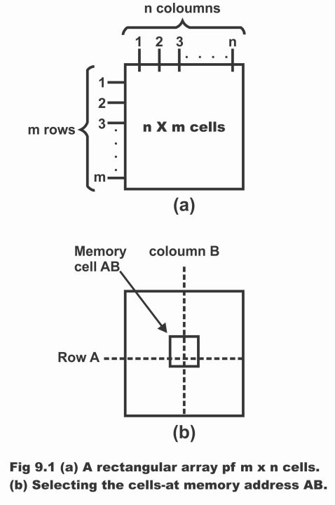
Basically, the control circuit fitted along memory array has been designed in such a manner that when one row out of entire rows and one column of all columns, is activated or energized (i.e. binary 1 signal provided on line), then the particular cell where intersection of two lines occurs or the point where two lines are cut or crossed, is selected. For example, in figure 9.1 (b), row line A and column line B have been shown as activated. As such, cell where intersection of row and column occurs, will be selected, by means of which data existing on the cell can be “read” and data present on the cell can also be “written”. This cell is called AB according to row and column selected. As such, AB means address of the cell.
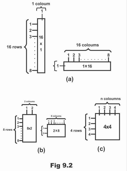
In figure 9.2, different rectangular arrays have been illustrated consisting of 16 cells. The total number of cells in all five conditions as shown in the figure, always remain 16. The 16 x 1 and 1 x 16 sequence shown in the figure (a) is exactly equivalent to 8 x 2 or 2 x 8 array in figure (b). Thus, a total of 3 different arrays are attained, wherein every array consists of an equal number of cells. The best of these arrays has been shown in figure (c) which comprises 8 address lines (i.e. 4 columns and 4 rows), (whereas figure (a) consists of a total of 17 address lines and figure (b) a total of 10 address lines). As this array or configuration consists of minimum address lines, therefore it is being used most extensively in industry. Therefore, square – shaped array (which comprises 4 lines and 4 columns, having a total capacity 4 x 4 = 16) as displayed in diagram (c) is preferred over rest of arrays. This array which has equal number of columns and rows, is known as “matrix addressing” whereas inversely, an array comprising multiple lines and a single column (as has been displayed via a 16 x 1 array in figure “a”) is generally known as “linear addressing”.
Figure 9.2
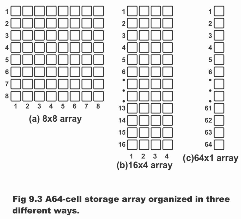
For further clarification, three different states or three different configurations of a storage array comprising 64 cells has been shown in figure 9.3. Every block existing in the memory array reflects a storage cell and identification of address or location of every cell is done by means of selection of a distinct row and a distinct column. In figure (a), an 8 x 8 array has been illustrated, which is also known as 64 – bit memory or 8-byte memory. In figure (b), 16 x 4 array has been depicted, which is a 16-nibble memory. Whereas in figure (c) a 64 x 1 array has been shown, which tends to be a 64 – bit memory (remember that 8 x 8 means a memory array which contains 8 columns and 8 rows. Similarly, 16 x 4 array means that number of rows is 16 whereas number of columns is 4 and 16 x 1 means an array in which number of rows is 16, however just one column exists in it). Further, identification of memory is performed by means of multiplying number of stored words with size of the words. For example, a 16K x 4 memory can store 16, 384 words (each word of which consists of 4 – bit). In fact, actual number of words tends to be according to the power of 2. In such a situation, it is 214 = 16,384. However, a thousand number practically is mentioned, which in this case is 16K.
Figure 9.3 – A 64 – cell storage array organized in three different ways
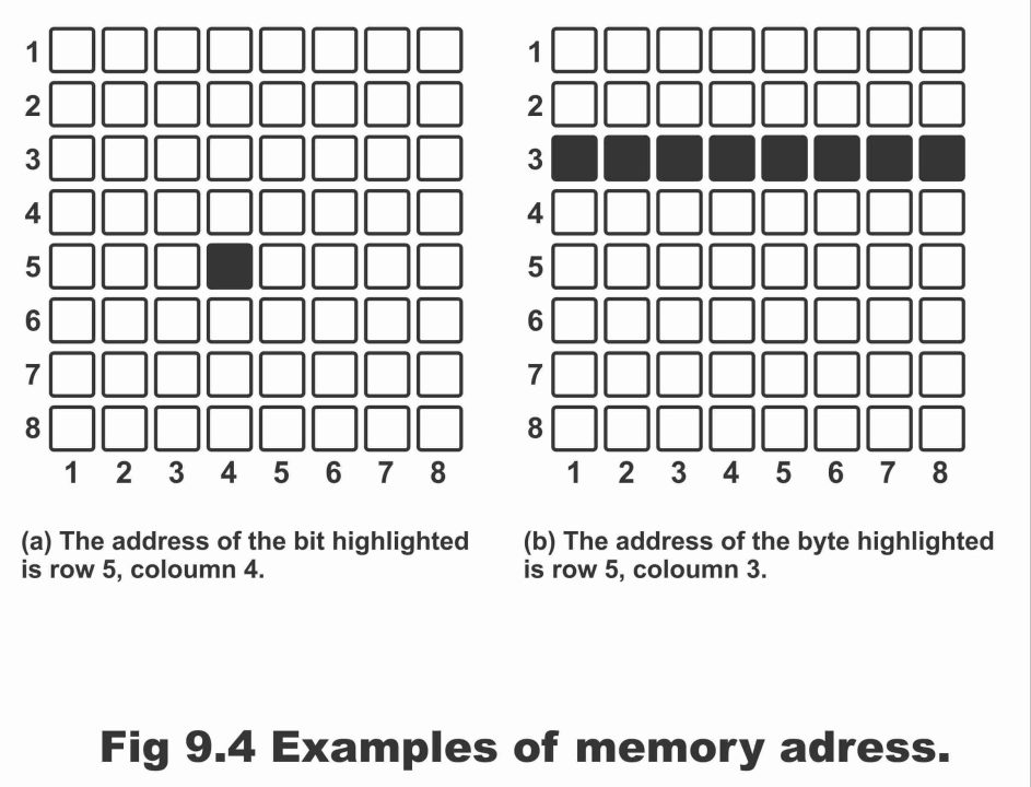
We know that location of a one unit of some data existing in a memory is known as its address. In figure 9.4 (a), bit – address existing in a 8×8 array has been illustrated with the help of a column and row, which signifies row number 5 and column number 4. While in figure (b), address of a byte (which is a sum or collection of 8 bits) has been displayed through row number 3 only. As such, it becomes clear from these figures that address depends on the point that from how many units of data memory has been configured. The capacity of a memory actually refers to total number of data units (which can be stored). For example, memory array capacity of a bit shown in figure (a) is 64 bits, whereas as memory shown in figure (b) has been arranged on the basis of byte, therefore capacity of this memory is 8 bytes, which is in fact equal to 64 bits. As a memory stores binary data, therefore data is entered into memory by means of a distinct address and whenever required, the data can be extracted or retrieved through this specific address.
Write operation is generally used in order to enter data on a specific memory address, whereas data is extracted from the specific memory address by means of read operation. As such, addressing operation which consists of both write and read factors, selects a particular memory address.
Figure 9.4 – Examples of memory address
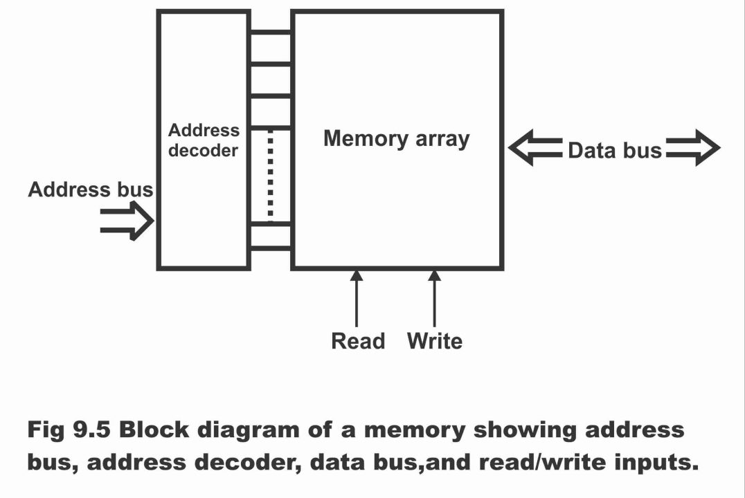
Data enters memory during write operation and exits from memory during the read operation. A set of lines is used in order to enter or eject data from the memory, which is known as data bus (i.e. set of lines through which data penetrates or leaves out of the memory, is called data bus). Data bus is bi-directional, as is obvious from figure 9.5. it means that data can process from either of these two directions (i.e. data can switch into or switch out from the memory via this bus or path). In case of a byte organized memory (memory arranged or arrayed with respect to bytes), the data base consists of eight parallel lines (i.e. one byte contains 8 bits), so that all eight bits of the selected byte may be transferred collectively to the memory in parallel form. Moreover, selection of address for write and read operation is done on the basis of a binary code, which is transmitted on the desired address by means of a set of lines. This set of lines is called address bus. Address code (which is in binary) is decoded (i.e. converted into decimal) via a decoder, as has been illustrated in the figure and as such, a proper address is selected. The number of rows in an address bus depends on memory capacity. For instance, a 4 – bit address code can select 16 locations (24) in memory, whereas an 8- bit address code can select 256 locations (28). The explanation of write and read operation under memory addressing, is as follows;
Figure 9.5 – Block diagram of a memory showing address bus, address decider, data bus and read/ write inputs.
The Write Operation
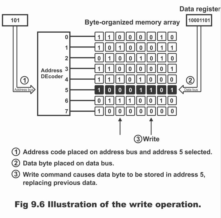
A basic write operation has been shown vide figure 9.6. In order to store a byte of data into memory, a code existing in the address register, is provided on address bus. Once address code is received on the bus, address decoder decodes this address (i.e. converts binary into decimal), on the basis of which selection of a specific location is made in the memory. Thus, a write command is received on memory (i.e. memory address is selected) and data bytes existing in data register, tend to store on the selected memory address via the data bus. As such, write operation is completed. It ought to be remembered that a when a new data byte is written on the memory address, stored data bytes or data available on this address, is lost or it becomes useless.
Figure 9.6 – Illustration of the write operation
The Read Operation
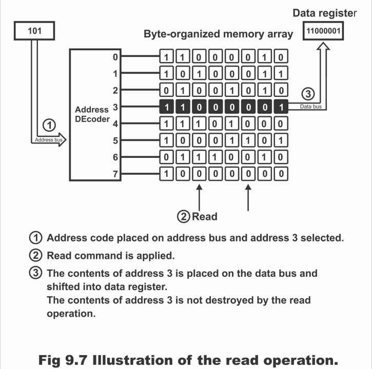
In figure 9.7, basic read operation has been illustrated. For read operation, once again a code is provided from address register to the address bus. This code is delivered on to decoder via an address bus, which decodes the code in order to select a specific location on the memory (i.e. it selects address or location wherefrom data has to be received or read). As such, memory receives a read command and a copy of the stored data bytes on selected memory address, is loaded on to data register via data bus. Thus, read operation gets completed. It must be remembered here that when a data byte is read through a memory address, the data byte remains stored on the specific address and it is not lost from its address.
Figure 9.7 – Illustration of the read operation
Previous Topic: Types of Memories: Magnetic and Solid state Memory in Digital Electronics
Next Topic: Read Only Memory (ROM) in Digital Electronics
For electronics and programming-related projects visit my YouTube channel.
Discover more from Electronic Clinic
Subscribe to get the latest posts sent to your email.
