Read Only Memory (ROM) in Digital Electronics
Last Updated on December 27, 2022 by Engr. Shahzada Fahad
Table of Contents
Read Only Memory (ROM)
Read only memory (which is also shortly known as ROM) is a kind of memory where in data can be stored or protected permanently and where from it is possible only to read this data (as can be implied from its name). In other words, a type of memory, where in data existing permanently on memory, can only be read and data can neither be erased nor any kind within the data, is possible (i.e. nothing can be written on this memory) is called a read-only memory (ROM). ROM is a non-volatile type of memory because the data stored on it remains fully protected in the event of a power breakdown. When ROM is being manufactured in the form of an integrated circuit chip, the manufacturer of the chip keeping in view the requirements of a consumer, stores data permanently on it as per standard specifications, and data gets protected on memory permanently (i.e. the user can neither erase nor edit this data later on). As this memory is in the form of a chip, and it is programmed by the manufacturer or factory, therefore it is also known as a Mask ROM(Read only memory) (remember that a computer program is called software, however, when a computer program or software has been stored on a ROM(Read only memory), it is known as firmware, because making any sort of changes on it, is no longer possible now). Normally, such type of data is stored on a ROM which are required recurrently. For example, tables, code converters or conversion, programmed instructions for operating a system, program language or machine language, operating system and character codes etc. It has to remembered that ROM is an internal memory of any computer system which can be read by only a microprocessor. The data stored inside a ROM is not lost or erased even if computer is turned off. As the initial costs of a ROM(Read only memory) is quite high, therefore it is always manufactured on large scale (because if initial manufacturing costs of any item are high, its price can be managed by means of producing that item on a large scale or in bulk quantity)
As read-only memory (ROM) is a semi-conductor memory, therefore bipolar technology (e.g. TTL) or MOS (metal oxide semiconductor) technology (wherein MOSFETs are used) are used for its production. The most significant MOS technologies include PMOS, NMOS, and CMOS. In PMOS, P channel FETs, and in NMOS N channel FETs whereas in CMOS (complementary metal oxide semiconductor) both P and N types of FETs are applied. However, due to a very high speed and very high density, NMOS has a predominant preference over PMOS in MOS technology. However, the application of CMOS within memory devices has increased tremendously these days. Most of the commercial ROMs are available in the form of a dual-in-line package (DIP). ROMs are available in low as well as in very high capacity. TTL74S370 is a very low-capacity unit, which consists of a 2048 – bit ROM(Read only memory) and 512 words consisting of 4 -bit, which may be stored on it (i.e. 512×4 = 2048). TMS47C512 is a high-capacity CMOS unit, wherein 65536 words consisting of 8 – bit, can be stored and its access time is 200 to 350 nanoseconds. Generally, such type of ROMs is used in personal computers. ROM(Read only memory) has the following types;
(1). PROM
(2). EPROM
The detail of these two types has been mentioned in the coming pages.
There are further two types of EPROM
(a). UV EPROM and (b). EEPROM
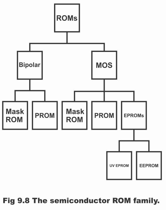
Remember that a Mask ROM(Read only memory) and a Programmable ROM or PROM(Programmable Read only memory), can be manufactured under any type of technology (bipolar or MOS) whereas EPROM (or Erasable PROM) is only and only just a MOS device. UV EPROM (or Ultraviolet EPROM) is a programmable ROM, wherein a user can electrically conduct programming according to his / her own sweet will or requirements. However, if the data which has been stored on it, is desired to be erased or wiped out permanently, a strong ultraviolet light has to be reflected on it for few minutes via a glass for the purpose. However, in EEPROM (electrically erasable PROM) the stored data can be erased or wiped out within a few milli- seconds time by means of applying a high-voltage pulse on the programming pins. In figure 9.8, a complete family of semiconductor ROM(Read only memory) has been demonstrated. Hence, a ROM consists of following characteristics;
(i). This memory is of a simple type
(ii). Its cost is low
(iii). Its speed is extremely high
(iv). It is a non–volatile memory
(v). Its construction or structure is simple and it can be manufactured in any technology e.g. diodes, transistors and MOS
The greatest disadvantage of a ROM is that it can only be read (read means reflection of contents of a memory location on a ROM’s output terminals) and no change is possible within it (i.e. it does not support the write facility, therefore transfer of data into memory from our end is not possible)
Construction of ROM(Read only memory)
We know that a ROM(Read only memory) is programmed permanently at the time of manufacturing, after which no changes are possible in its programming or data stored on it. A ROM consists of bipolar or MOS, however ROMs can also be fabricated by means of using diodes instead of transistors or MOSFETs. In such a case, ROM(Read only memory) becomes unipolar.
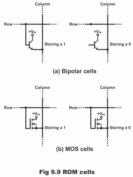
In figure 9.9 (a), bipolar ROM cells have been illustrated. If a connection exists between row line and transistor’s base, this location or address is denoted by 1 (i.e. wherever transistor connection inside a bipolar ROM has been done in this manner, binary 1 stores on that location) because when row line is high, transistor’s bases connected with these row lines power on and render the corresponding column lines high i.e. 1. However, against it, if an address is applied on row, then such row/column junctions, where no base connections exist, all lines remain low or 0.
In figure (b), ROM cells composed of MOS have been represented. Principally, these cells also resemble bipolar cells, except that these cells are prepared from MOSFETs (metal oxide semiconductor field effect transistors). Here too, binary 1 or binary 0 stores permanently as a result of the existence or non-existence of gate connections respectively on the junction. This has been illustrated in the figure given below;
Figure 9.9 – ROM cells
Programming of ROM(Read only memory)
For the sake of simplicity and better understanding, here only unipolar ROM (i.e. ROM consisting of diodes) is being considered and discussed. Suppose that we want to design a ROM which comprises 8 memory locations and 4 data lines (i.e. 8 x 4 ROM). For this purpose, draw 8 horizontal lines which represent 8 memory locations. Now draw 4 perpendicular lines above these 8 straight or horizontal lines, which behave here like data output lines. This has been elucidated in figure 9.10. Assume that we want to do ROM programming according to the contents given in the table 9.11. For this end, diode method is used for the purpose of storing data. According to the data given in the table, fix a diode at locations wherever logic 1 exists.
Figure 9.10
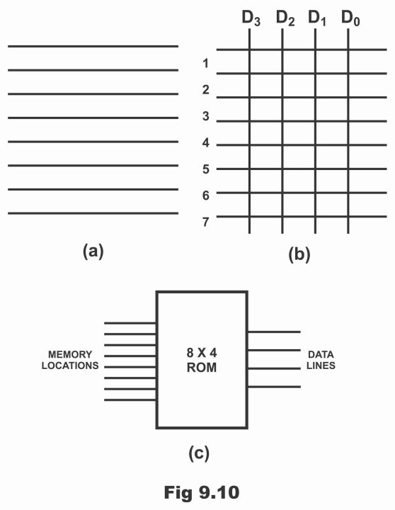
Figure 9.11 – Diode ROM
| Register | Address | Word |
| R0 | 0 | 0111 |
| R1 | 1 | 1000 |
| R2 | 2 | 1011 |
| R3 | 3 | 1100 |
| R4 | 4 | 0110 |
| R5 | 5 | 1001 |
| R6 | 6 | 0011 |
| R7 | 7 | 1110 |
Working
In figure 9.12, a simple diode ROM(Read only memory) has been illustrated, every straight or horizontal line of which represents a register or a memory location. According to this figure, R0 register consists of three diodes, R1 register one diode, R2 register three diodes, R3 register two diodes, R4 register four diodes, R5 register two diodes, R6 register two diodes and R7 register three diodes. If the figure is prudently observed, it becomes evident that anode of a diode has been connected with row whereas cathode of every diode has been connected with column line. The output of this ROM is as follows;
Figure 9.12 – Simple Diode ROM
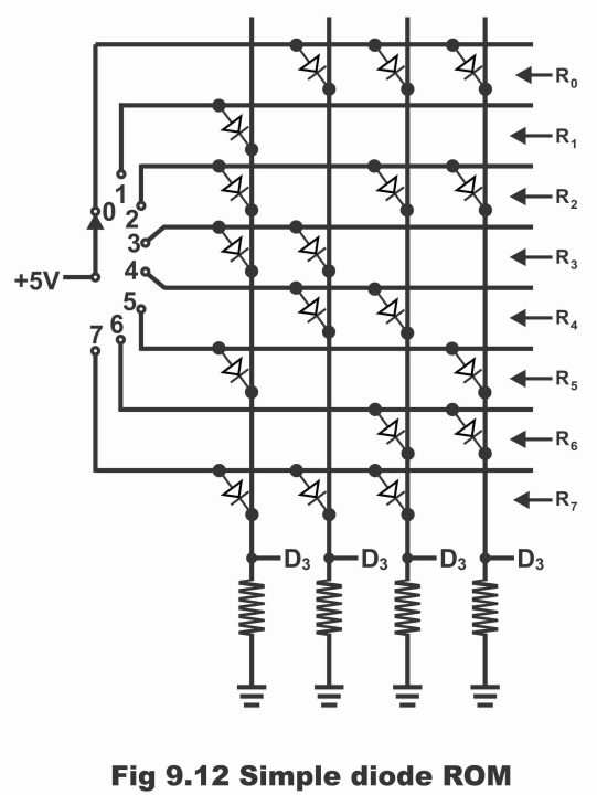
When input is brought on position 0 by means of spinning the rotary switch, then high voltage (+5V) are received on all three diodes present on the R0 register or memory location. As a result, all these three diodes turn on. Whereas rest of the diodes present on ROM tend to remain off. It means that a high output is received on D0, D1 and D2. Resultantly, the following word is stored on memory location or register R0;
D = 0 1 1 1
When switch is rotated and set on position 1, then the sole diode mounted along register R1 or on this line, conducts. As a result, D3 output becomes high (because this diode has been connected with D3 data line). As rest of the diodes remain off under such a condition, therefore following output is obtained from ROM;
D = 1 0 0 0
Thus, contents of memory location 1 are 1 0 0 0. Remember that if one LED each is fitted along outputs D0, D1, D2 and D3, then if any one of these four outputs get high, its corresponding LED will be illuminated.
Similarly, it is also possible to read contents or stored data of other memory locations by means of changing switch positions (every new position of a rotary switch is known as address). These contents have been illustrated via a table in figure 9.11.
Selection of ROM Address
Contents and address are two separate things. As has been illustrated by the table, address of a memory location equals to the word being stored on a register. This is the reason address of register R0 is 0, however its contents are 0 1 1 1. Similarly, R1 address is 1, but the value of its contents is 1 0 0 0. If the ROM(Read only memory) circuit is designed through discrete components, then contents of any memory location can be modified by means of injecting or emitting a diode from the circuit. However, it is not possible to do so in an integrated circuit (because all ROMs are in the form of integrated circuit chip). As manufacturers store data permanently in a ROM during its fabrication process, that’s why its programming cannot be transformed (i.e. as diode is being permanently fixed in a ROM, therefore neither a diode can be inserted into an IC nor switched out from the ROM. Hence, words are constantly or permanently stored on a ROM)
Thus, by means of applying voltage on different memory locations of a ROM, data exiting there can only be read. It should be kept in mind that ROM can be applied address of any size. For example, a ROM with 256 memory locations consists of decimal addresses ranging from 0 through 255. Similarly, a 1024 memory locations ROM, consists of decimal addresses from 0 through 1023.
On-Chip Decoding
As selection of readable data existing in a ROM(Read only memory) totally depends on the number of address line rows and as too many address lines render circuit complicated, therefore instead of a selector switch, all IC manufacturers use a 3 x 8-line binary to decimal decoder (which is known as on – chip decoding) for selection of memory locations, by means of which 8 address lines decrease down to just 3 lines. This has been showed via figure 9.13. According to this diagram, the presence of diode means 1 whereas the non-presence of the diode means 0. These diodes can also be replaced with MOSFETs.
Figure 9.13 – ROM with on-chip decoding
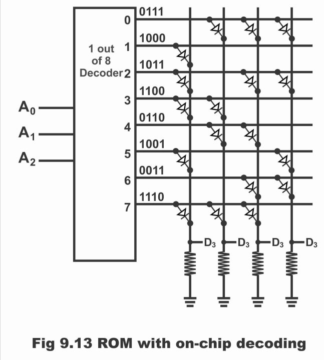
In these figure, three inputs pins A0, A1 and A2 are visible, through which any sort of data stored on a memory can be read by means of providing address. When these pins provide binary address of a stored word, then a 1 of 8 decoder (i.e. a decoder which selects just one of eight outputs) renders output of just one register out of all registers or memory locations, high. For example, suppose that we want to read data on address 100 or if address value is binary 100, i.e.
Address = A0 A1 A2 = 100 … (decimal 4)
Then, binary to decimal decoder provides high voltage on register R4. ROM output under such a situation, will be as follows;
D = D0 D1 D2 D3
D = 0 1 1 0
If the address word is changed to binary 110, then
Address = 110 … (decimal 6)
In such a situation, contents of memory location 6 can be read, value of which is as follows;
D = 0 0 1 1
In figure 9.14, the circuit shown is a 32 – bit ROM (i.e. 8 words x 4bits) which consists a total of 8 words, whereas each of its word contains 4 bits. This circuit has three address (input) lines and four data (output) lines. As compared to commercially available ROMs, it is a very low-capacity ROM.
Figure 9.14 – ROM with on-chip decoding
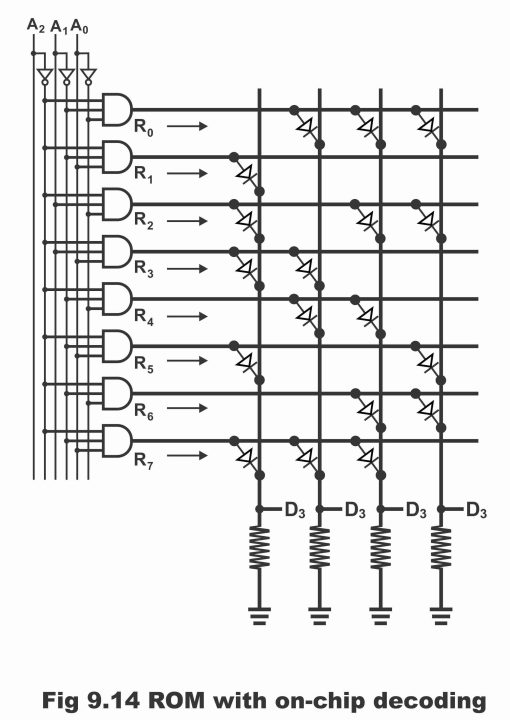
It must be remembered that in case of an on–chip decoding, “n” address lines can select “2n” memory locations. For example, we need 3 address lines in order to read 8 memory locations, as is evident from figure 9.14. Similarly, 4 address lines can elucidate 16 memory locations and as such 256 memory locations can be read via 8 address lines.
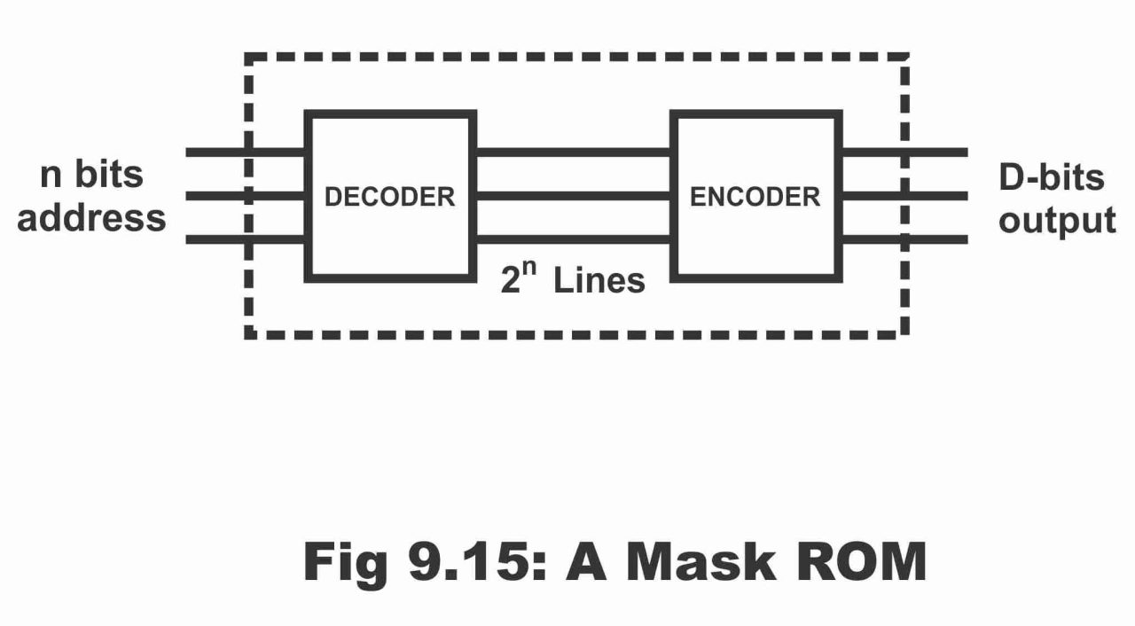
The ROM circuit shown in figure 9.15, is actually a combination of two logic circuits (an encoder and a decoder, i.e. ROM is fabricated by means of mounting an encoder and thereafter fitting a decoder), where in the mounted decoder (binary to the decimal converter) receives address consisting of 8 – bits and selects 2n memory locations on this basis. These selected 2n output lines are received on encoder (decimal to binary converter) which provides output in the form of D bits. This has been illustrated via figure 9.15.
Figure 9.15 – A Mask ROM
Capacity Of ROM:
Capacity means total number of stored locations. ROM capacity is represented in the form of code number. e.g. 2316. Here, the ROM(Read only memory) code is 23, whereas 16 is its capacity. If 16 is divided by 8, then 2316 code ROM capacity becomes 2KB. i.e.;
16 / 2 = 2KB
As such, capacity is equivalent to the following;
Capacity = Memory locations x Data Lines
Previous Topic: Memory Addressing: Writing And Reading Operation in Digital Electronics
Next Topic: Programmable Read Only Memory or PROM in Digital Electronics
For electronics and programming-related projects visit my YouTube channel.
Discover more from Electronic Clinic
Subscribe to get the latest posts sent to your email.