Programmable Read Only Memory or PROM in Digital Electronics
Last Updated on December 27, 2022 by Engr. Shahzada Fahad
Programmable Read Only Memory or PROM
Programmable read only memory (which is shortly known as PROM) is a type of a read-only memory (ROM) which is available in blank form, without any sort of programming having been done on it and wherein a user or customer can undertake programming just once according to his / her liking or needs. In other words, ROMs which are available in a blank or non-programmed form and in which data can be stored only once according to ones’ own needs or will, is called PROM(Programmable read only memory).
The instrument, which is used for programming purposes in a PROM(Programmable read only memory), is known as a PROM programmer, by means of which a user or customer burns or opens fusible links present on bit locations inside a PROM (programming of which is required to be undertaken) according to his requirements (for storing 0s) via applying a high current. It ought to be remembered here that non – existence of fusible link reflects binary 0 and presence of fusible link reflects binary 1 programming. This method of programming by means of burning fusible links, is called burning- in or fusing process and that’s the reason PROM(Programmable read only memory) is also known as a “Fusible Link PROM”. Remember that once the programming process has been completed through fusing or burning, thereafter programming carried out within a PROM(Programmable read only memory) becomes permanent (i.e. stored data in a PROM cannot be modified thereafter). In other words, PROM’s fusing process is irreversible, which cannot be changed subsequently.
Like ROM(Read only memory), PROM(Programmable read only memory) is also manufactured on the basis of bipolar or MOSFETs technology and the basic concepts related to the components being used in the construction of both, are also same (i.e. ROM or PROM whether manufactured via a bipolar or MOS technology, they operate just like a diode).
The designing technique of a PROM(Programmable read only memory) is just similar to that of a ROM, except that every memory cell of a PROM comprises of a diode and a fuse mounted along the diode on a series. By every memory cell consisting of a diode, we mean that under normal conditions, binary 1 is stored on all these cells (i.e. all cells are on logic 1 state). However, cell where binary 0 digit is required to be stored during a programming process, an appropriate quantity of current is being passed through fuse (which is located on diode series), as a result of which fuse dissolves and cell’s circuit opens up (i.e. current flowing path between fuse and diode opens, as a result of which diode’s connection existing on the cell, comes to an end). Resultantly, binary 0 stores on the cell with an open fuse or fusible link. While all memory cells, which have fuse in a proper condition (i.e. non – melted) reflect binary 1 storage on it.
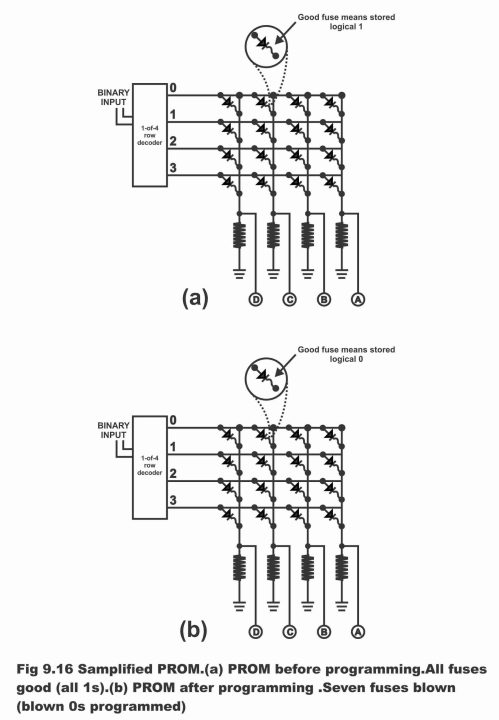
In figure 9.16 (a), a simple PROM has been illustrated prior to its programming. This figure reflects a 16 – bit (4×4) PROM. It is obviously clear from the figure that its every memory cell contains a diode and a good fuse. Here “good” means that logical 1 is stored on every PROM cell. It is such a condition, where practically no programming can possibly be carried out on this PROM.
In figure (b), PROM has been illustrated in a post-programmed state. According to the figure, 7 zeros have been programmed within it. In this figure, 7 fuses within different cells can be seen having been blown up. Programming is conducted in PROM(Programmable read only memory) when tiny fuses in a diode series on the desired cells, have been blown (i.e. they melt down as a result of passing of an extensive or extremely high current). In such a scenario, diode circuit becomes incomplete i.e. memory cell where fuse has been melted, diode (which has been mounted on fuse series), stops working in that cell (or it turns off). Memory cell, diode circuit of which is off, binary 0 stores permanently on to it (or a logical 0 state prevails permanently on it) as can be seen in the figure. As fuses which have been installed on a PROM memory cells, have permanently been diffused or melted after its programming, therefore it is not possible to reprogram it i.e. programming is possible just once within a programmable read only memory.
Figure 9.16 – Simplified PROM (a). PROM before programming. All fuses good (all 1s). (b). PROM after programming. Seven fuses blown (7 0s programmed)
In figure 9.17, a PROM’s simple programming setup has been illustrated. For programming purposes, first of all, an address is designated by means of setting a switch on the address lines, and then a pulse is exerted on these output lines via a pulse generator according to bit locations, where zeros (0s) are desired to be stored. These pulses melt or dissolve fusible links, and as a result, the desired bit pattern is designed. After this, the next address is selected and as such, the entire process is repeated once again. It is to be reminded here that such an arrangement or series occurs automatically, by means of a software-driven PROM programmer. PROMs are available in the market in the 25XX series.
Previous Topic: Read Only Memory (ROM) in Digital Electronics
Next Topic: Erasable Programmable Read Only Memory (EPROM) in Digital Electronics
For electronics and programming-related projects visit my YouTube channel.
Discover more from Electronic Clinic
Subscribe to get the latest posts sent to your email.