Microprocessor Operation or Function in Digital Electronics
Last Updated on April 18, 2023 by Engr. Shahzada Fahad
Microprocessor Operation or Function
The operation or function of a microprocessor has been illustrated vide figure 11.10. The following operation occurs in this example;

1). Press “A” key on the keyboard (input is provided on microprocessor through this action)
2). The word “A” stored on the memory (this action is called storage)
3). The word “A” prints or is displayed on the CRT screen (this action signifies device output)
The input–store–output method illustrated in this diagram, represents the entire operation of a microcomputer system, however electronic hardware used in this system consists of complex and complicated circuits.
Figure 11.1- – An example of a common input–store–output microprocessor
In order to understand input-store -output method of a microcomputer, the sequence or configuration of these operations has been illustrated by means of a detailed block diagram in figure 11.11. In order to understand this operation, first we carefully analyze program contents sections of the memory.
It is worth mentioning here that instructions within first six memory locations have been pre – loaded. The instructions (as has been illustrated through the diagram) existing on this memory are as follows;
- Input data is received from input port 1
- Stored data of port 1 on data memory location 200
- Output data is transmitted on output port 10
Figure 11.11 – sequence of microcomputer operation in executing the input–store–output program
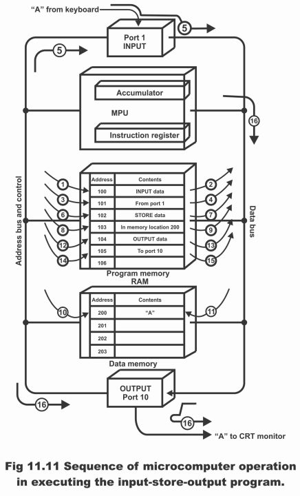
It must be indoctrinated in mind that the aforementioned program contains just three instructions. In figure 11.11, these 3 instructions appear in the form of six instructions. This is because instructions on program memory are divided into different segments. The first part of instruction 1 as narrated above is related to the input data, whereas 2nd segment of this instruction tells wherefrom the data comes (from port 1). First part (action part) of this instruction is called operation, whereas its 2nd part is known as operand. Operation and operand store or appear on different or separate program memory locations, as has been indicated in the figure. The first part (i.e. input data or output operation) of the first instruction exists on location 100 in the program memory whereas its 2nd part (operand or port 1) exists on location 101, which tells that information is received from this input.
In figure 11.11, two new parts or segments have been illustrated inside a microprocessor unit (MPU). These two new parts are called registers. These special registers are called accumulators and instruction register.
When the word “A” is entered into the keyboard through a microprocessor, what is the input–store–output operational sequence on this word in a microprocessor? This has been illustrated by means of an example given in figure 11.11. The instructions and data flow operation can be comprehended with the help of round circles illustrated in the figure. Remember that the microprocessor unit (MPU), is the center for the entire data transfer and operations (i.e. MPU is a center for carrying out all operations and data transfer)
According to figure 11.11, operations of the microprocessor’s functions are carried out in the following manner;
- MPU transmits address 100 on Bus address. The control line enables read input on program memory IC. This step has been represented by means of an encircled 1 in the figure.
- Program memory transmits first input data instruction on data Bus and MPU receives this coded message. This input data instruction transfers on to a special memory location within a MPU, which is called an instruction register. MPU decodes this input data instruction and determines whether input data instruction (i.e. first instruction) requires operand.
- MPU transmits address 101 on the Address Bus. The control line enables read input of program memory in order to operate.
- Program memory provides the database to Operand (from port 1). Operand existed in program memory at address 101. The database fetches this coded message (i.e. address for port 1) and transfers it to the instruction register. Now MPU decodes the whole instruction (input data from port 1).
- MPU uses an address Bus and control lines to open the input unit, port 1. “A” shifts toward the MPU accumulator in a coded form and stores there. It must be remembered here that MPU always functions according to the Fetch – Decode – Execute configuration or sequence. First, it fetches instructions from program memory. In the 2nd step, MPU decodes these instructions. In the 3rd step, MPU executes these instructions (i.e. it acts according to these instructions)
- MPU addresses location 102 on the Address Bus. MPU uses control lines in order to enable read input on the program memory.
- Code is transmitted for data instruction stored on the data bus, which MPU fetches and transfers onward to the instruction register.
- MPU decodes stored data instruction and determine whether it needs an Operand. Then MPU addresses the next memory location 103 and enables or activates program memory read input.
- An “in memory location 200” code is provided on the data Bus by means of program memory. MPU accepts this Operand and stores it in the instruction register. As such, the entire stored data on memory location 200 is fetched from the memory and decoded.
- After fetch and decoding, the execution operation starts. MPU transmits address 200 on to the address Bus enables or activating the write input of the data memory.
- MPU transmits stored information on the accumulator to memory via the data Bus. As such, data bus receives “A” and gets it written on location 200 existing inside the data memory. Thus, rest of the instructions are also executed. The contents present on an accumulator do not lose as a result of this storing process and stored “A” on the accumulator still exists in its coded form.
- Similarly, MPU now fetches the next instruction. This location addresses location 104 and enables read input of program memory.
- The code for output data instruction is transmitted on MPU via data Bus, which fetches these instructions and transmit it on the instruction register. MPU decodes these instructions and determines whether it needs an Operand.
- MPU sends address 105 on the address Bus and enables read memory of program input.
- Program memory sends code on MPU for Operand (to port 10) via the data Bus. MPU fetches this code on instruction register or MPU receives this code and transmits or sends it to instruction register.
- MPU decodes whole instruction (“output data to port 10”) and then activates port 10 for output unit by means of using address bus and control lines. Then MPU transmits word “A” on to data Bus (which is still stored on the accumulator) and thus, word “A” transfers on CRT monitor (or displays on monitor) set outside the output port 10.
It becomes clear from the aforementioned explanation that MPU is center of all operations and it controls entire operations. MPU always operate in fetch -decode – execute sequence, however, actual operation of the MPU system can be understood by means of the list given on its program memory. Normally, sequence of instructions tends to be 100, 101 and 102 etc. Three instructions given in the afore-mentioned example fetch, decode and execute in a few milliseconds or in a time even less than this. The advantage of a system organized on the basis of MPU is that they are fast in its operation, further flexibility also exists in them (i.e. their re-programming is possible for carrying out multiple tasks). Remember, a faster MPU-based system transfers information just in accordance with the procedure mentioned in the aforementioned detail (as can be seen in figure 11.11). However, the operation of some microprocessors may be slightly different. Probably, major difference occurs in the input and output sections. For this purpose, further steps are essential to be taken for operating input-output sections in an appropriate manner.
Previous Topic: Type of Electronic Machine in Digital Electronics
Next Topic: Microprocessor Architecture / Organization in Digital Electronics
Discover more from Electronic Clinic
Subscribe to get the latest posts sent to your email.