Synchronous Counter in Digital Electronics with circuit Diagram
Last Updated on December 2, 2022 by Engr. Shahzada Fahad
Synchronous Counters
The synchronous counter is a counter where in all clocks inside flop-flops are shorted (i.e. all flip-flops clocks are controlled simultaneously by means of a single clock pulse or every flip-flop receives an equivalent clock pulse). In other words, counters where in all flip-flops are synchronized or harmonized (i.e. coherent with a single clock pulse) through a common clock pulse (which is required to be counted), are called synchronous counters. Remember that all flip-flops are connected together in a parallel fashion with respect to the clock pulse in such types of counters, owing to which, an equal clock pulse is received on all flip-flops. Therefore, these types of counters are also called parallel counters. As all flip-flops of such counters operate together due to a parallel clock pulse, or they change their states all together, therefore circuit’s overall propagation delay time is equivalent to the propagation delay time of just one circuit. Therefore, as a result of a low propagation delay time of this counter (relative to an asynchronous counter), its counting speed is higher.
We know that in asynchronous or ripple counters (which have been discussed above) all flip-flops have been inter-connected in a manner that output of one flip-flop becomes input for another other flip-flop. Whereas pulses coming from clock (which are desired to be calculated) are only exerted on the first flip-flop. The effect of these pulses is felt on all flip-flops in a serial fashion. As all flip-flops in a ripple counter are not coherent or synchronized with a common clock pulse or these flip-flops are not controlled via a common pulse, therefore ripple counter is also known as an asynchronous counter. Further, total propagation delay time of a ripple counter is equal to the sum of individual propagation delay time of all flip-flops existing within the counter. As such, its speed is low (as compared to a synchronous counter) as a result of a high overall propagation delay time.
In figure 8.4, a 2-bit synchronous binary counter has been represented, which consists of two JK flip-flops and a series of clock pulses. It is obvious from the figure that every flip-flop has been receiving an equivalent clock pulse, as result of which, both flip – flops change their state simultaneously. According to the diagram, only input J0K0 of the first flip-flop FF0 has been connected with binary 1 or high, so that the flip-flop may operate consistently. Therefore, whenever clock pulse is received, first flip-flop of this counter changes its state just similar to the first flip-flop of a ripple counter. However, J1K1 input of FF1 flip-flop is controlled with FF0 flip-flop’s normal output Q0. It means that FF1 flip-flops change its state only when normal output of FF0 flip-flop is binary 1. In order to fully comprehend the operation of this type of counter, we need to be it bear in mind that when positive edge of a clock pulse strikes, flip-flop tend to toggle at that time. The operational mechanism of a 2-bit synchronous counter is as follows;
Figure 8.4-a 2-bit synchronous binary counter
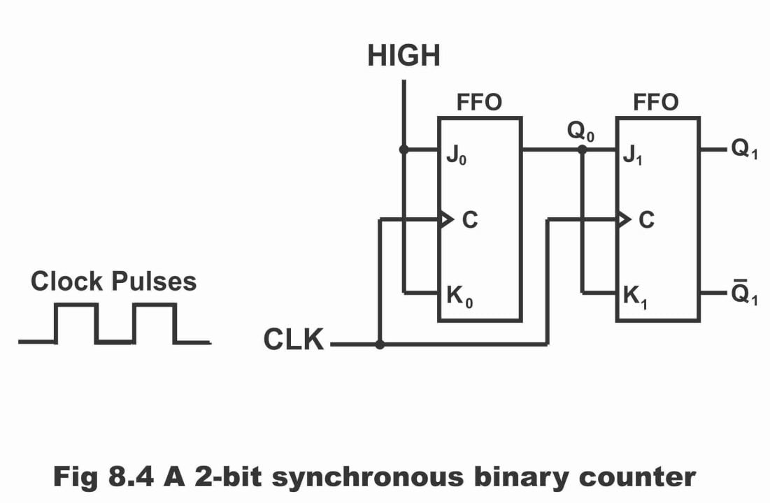
(1). In the beginning, it is presumed that the counter is on binary 0 state (i.e. both flip-flops are set initially). When positive edge of the first clock pulse is applied on the counter, FF0 flip-flop toggles (i.e. change its state) as a result of which, it will become set and its output Q0 will turn out to be high after the propagation delay time. In such a situation, when flip-flop FF0 toggles, and its output changes a bit belatedly due to the propagation delay, then what impact will be exerted on flip-flip FF1 when positive edge of the first clock pulse is applied on it? In order to understand this thing, we will have to see input states of FF1. At that time, flip-flop inputs J1 and K1 both are low, because owing to a propagation delay, both inputs are still connected to Q0. Although, positive edge of the clock pulse is continuously being received on flip-flop FF1 (remember that flip-flop FF1 will change its state only when both its inputs i.e. J1 and K1 or normal output of FF0 flip-flop is binary 1 and FF0 flip-flops’ output state will change following this propagation delay). When positive edge of the first clock pulse is received, then FF0 flip-flop toggles and sets as a result of high K0 and J0 inputs. However, as a result of low J1 and K1 inputs, no change occurs on the state of flip-flop FF1 (because both of its inputs are connected to Q0 and Q0 state which is binary 0 at that time, changes only after the propagation delay time of FF0 flip-flop). Therefore, after first positive edge of the clock pulse (CLK1) has been received, output of both flip-flops will be as under;
Q0 = 1 and Q1 = 0
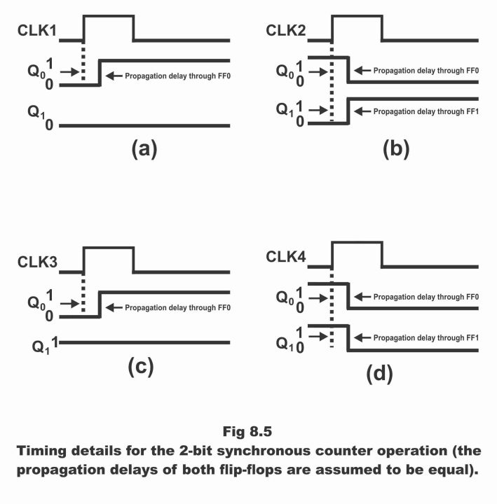
The timing details of this part of counter’s operation has been shown in figure 8.5 (a). Remember that afore- mention two states represent binary 1.
Figure 8.5-timing details for the 2-bit synchronous counter operation (the propagation delays of both flip-flops are assumed to be equal).
(2). When positive or leading edge of the 2nd clock pulse (CLK2) is received, then FF0 flip-flop toggles, its output Q0 changes from its previous state binary 1 to binary 0 or it becomes low. As FF1 inputs J1 and K1 on this clock pulse triggering edge have been changed or become high after the propagation delay time of first flip-flop FF0, or these two inputs are on its high state at that time (i.e. Q0 = 1), therefore FF1 flip-flop toggles on the 2nd clock pulse and its output Q1 becomes high. Thus, after CLK2;
Q0 = 0 and Q1 = 1
Afore-mentioned two states on the outputs of both flip-flops represent binary state 2. The timing detail of these states has been illustrated in figure (b).
(3). When leading edge of the 3rd clock pulse (CLK3) strikes, then FF0 flip-flop toggles once again and sets (i.e. Q0 = 1) and at that moment, FF1 flip-flop remains on its previous state (i.e. Q1 = 1) because both its J1 and K1 inputs are low i.e. Q0 = 0. It ought to be remembered that state of this flip-flop changes only when both of its inputs are high, as has been explained above. After this triggering edge, following states occur on outputs of both the flip-flops;
Q0 = 1 and Q1 = 1
Afore-mentioned two states represent binary 3. Timing details of these states has been shown in figure ©.
(4). Finally, when leading edge of the 4th clock pulse (CLK4) is received, outputs Q0 and Q1 of both flip-flops tend to turn low, because toggle conduction takes place simultaneously on both J and K inputs of these flip-flops. This has been explained via timing details in figure (d). As such, this 2-bit counter returns back on its initial state after application of 4th clock pulse i.e.
Q0 = 0 and Q1 = 0
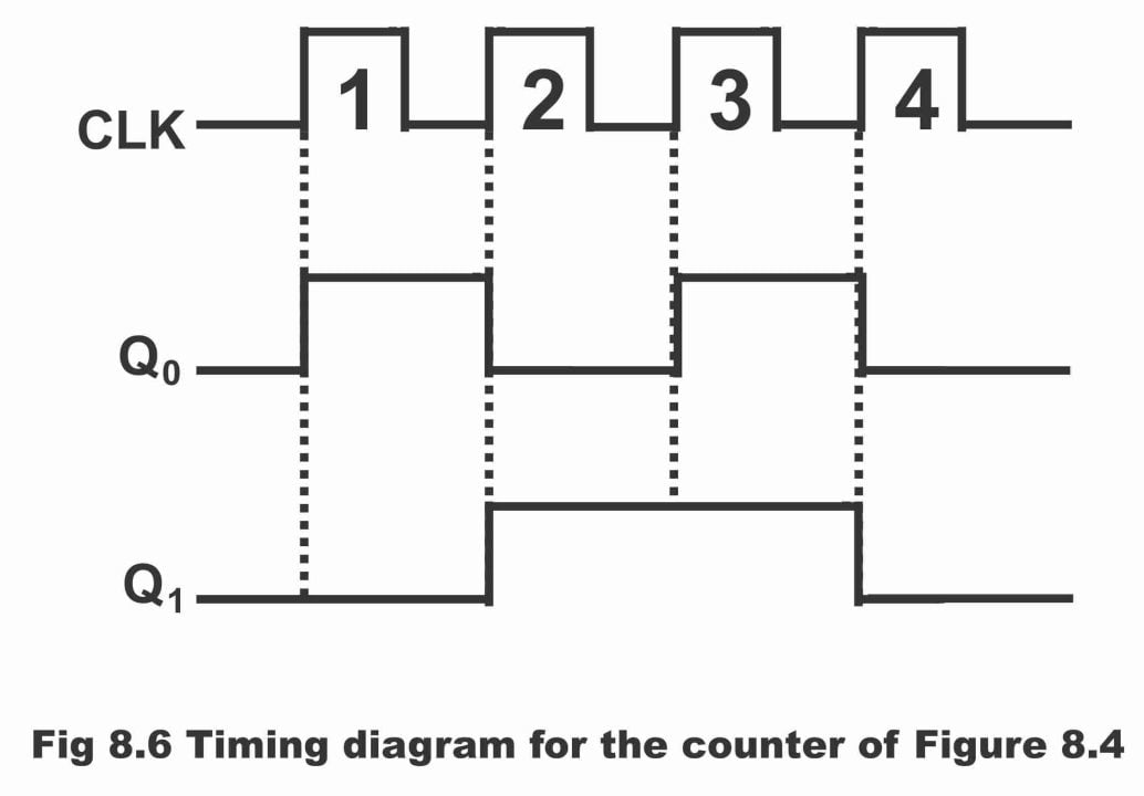
The complete timing diagram of this counter has been reflected in figure 8.6. The propagation delays occurring within this counter have not been displayed. Although, delays are important for operation in synchronous counters, however for the sake of simplicity, these are not shown in overall timing diagram, so that timing diagrams can be read and comprehended easily.
Figure 8.6-timing diagram for the counter of figure 8.4
In figure 8.7, logic diagram of a 3-bit (mod – 8) synchronous binary counter and in figure 8.8 its timing diagram has been illustrated. It is obvious from logic diagram of the counter that clock has been connected directly with the clock input of every flip-flop (i.e. clock inputs are inter-connected in parallel). In the table shown in figure 8.9, counting sequence (i.e. counting arrangement of the counter) of this counter has been illustrated. The counter’s operation can easily be understood as a result of a little consideration on the table. The column Q0 given in the table, is binary 1s column and flip-flop FF0 conducts counting for this column. Column Q1 is binary 2s column and flip-flop FF1 performs counting for this column. Column Q2 is binary 4s column and flip-flop FF2 undertakes counting for this column.
Figure 8.7-A 3-bit synchronous binary counter
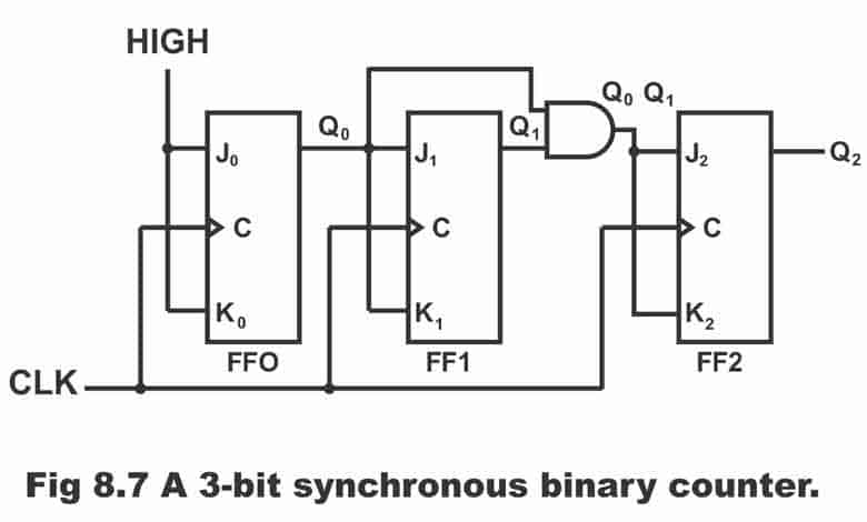
Figure 8.8-timing diagram for the 3-bit counter
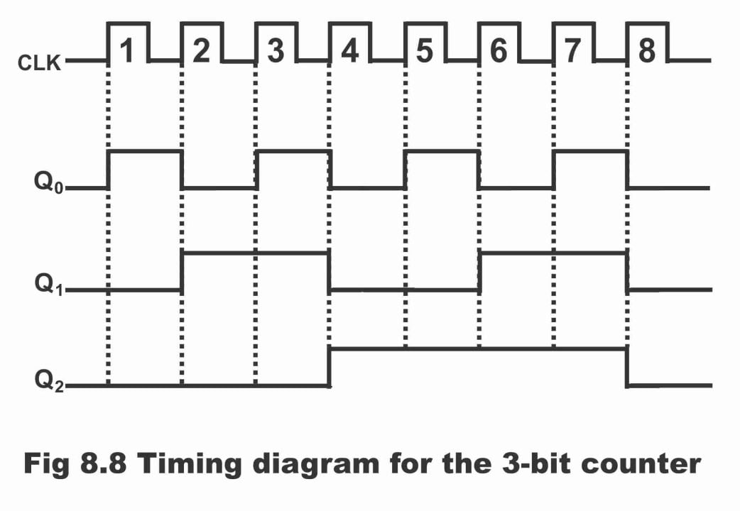
Figure 8.9-timing sequence for a 3-bit binary (synchronous) counter
| Rows | Number of Clock Pulses | Binary Counting Sequence | Decimal Count | ||
| Q2 | Q1 | Q0 | |||
| 1 | 0 | 0 | 0 | 0 | 0 |
| 2 | 1 | 0 | 0 | 1 | 1 |
| 3 | 2 | 0 | 1 | 0 | 2 |
| 4 | 3 | 0 | 1 | 1 | 3 |
| 5 | 4 | 1 | 0 | 0 | 4 |
| 6 | 5 | 1 | 0 | 1 | 5 |
| 7 | 6 | 1 | 1 | 0 | 6 |
| 8 | 7 | 1 | 1 | 1 | 7 |
| 9 | 8 | 0 | 0 | 0 | 0 |
First of all, look at the Q0 column given in the table. After a careful observation, it becomes clear that Q0 tends to change on every clock pulse, as a result of which counter shifts from its original state to the final state and then from final state, it returns back to its original state. In order to generate this operation on counter, J0 and K0 inputs of flip-flop is constantly maintained high (as is evident from the logic diagram) so that the flip- flop remains in the toggle mode. It is also evident from the table that every time when value of Q0 is binary 1, thereafter Q1 treads on its reverse mode i.e. (binary 0). This change takes place on CLK2, CLK4, CLK6 and CLK8. As a result of clock pulse 8 (i.e. CLK8) counter enters recycle state (i.e. counter re- starts counting). In order to initiate this operation, Q0 is connected with J1 and K1 inputs of flip-flop FF1. When value of Q0 is 1, and clock pulse occurs at that time, then FF1 enters into toggle mode, as a result its state undergoes a change. However, at other times, when value of Q0 is 0, no change takes place in FF1 and it tends to sustain its present state.
Now we see how does FF2 changes its state in accordance with a binary sequence during suitable times. If column 2 given in the table is discreetly pondered upon, it becomes obvious that Q2 state changes when both Q1 and Q0 are high. This condition is achieved by means of installing an AND gate before J2 and K2 inputs of FF2 flip-flop (remember that when both inputs Q0 and Q1 of AND gate are high, its out is also high at that time). Whenever both Q0 and Q1 are high, then AND gates output become high too, owing to which FF2 flip-flop J2 and K2 inputs also turn high. Thus, FF2 toggles upon striking of clock pulse (i.e. changes its mode). During rest of the times, J2 and K2 inputs of FF2 remain low as a result of low AND gate output. Consequently, FF2 does not change its state. Thus, operational detail for a 3-bit synchronous counter is as follows;
(1). Initially let us assume that all flip-flops within the counter are reset due to non-presence of a clock pulse. This has been illustrated vide first line (row) of the table. In such a situation, counter’s output is as follows;
Q2 Q1 Q0 = 0 0 0 (decimal 0)
(2). On receiving the first clock pulse via clock (as has been indicated in 2nd row of the table) all flip-flops receive this clock pulse simultaneously or at a time. However, just FF0 flip-flop toggles as a result of this pulse, because it is the only flip-flop both J0 and K0 inputs of which are high. Thus, FF0 shifts from binary 0 to binary 1 (i.e. it sets). Thus, counter represents following output;
Q2 Q1 Q0 = 0 0 1 (decimal 1)
(3). When the clock pulse 2 strikes, only two flip-flops (FF0 and FF1) of the three toggles, because both their inputs are high at that time. Therefore, FF0 flip-flop changes its state from binary 1 to binary 0 (i.e. it resets), whereas FF1 flip-flop changes its state from binary 0 to binary 1 (as depicted via line number 3 of the table). Thus, following output results;
Q2 Q1 Q0 = 0 1 0 (decimal 2)
(4). On the arrival of clock pulse 3, all three flip-flops receive this pulse, however only one of the three flip-flops (i.e. FF0) toggles and gets set (or FF0 state changes from o to 1). This has been illustrated vide line number 4 of the table. As such, output is obtained as follows;
Q2 Q1 Q0 = 0 1 1 (decimal 3)
(5). When clock pulse 4 strikes, all flip-flops toggle and come on their opposite or reverse states. i.e. FF0 becomes 0 from 1. FF1 state changes from 1 to 0 and FF3 state turns 0 to 1. This has been depicted in line number 5 of the truth table. As a result, following output is obtained;
Q2 Q1 Q0 = 1 0 0 (decimal 4)
(6). As clock pulse 5 strikes with the counter, all flip-flops receive this pulse simultaneously, however mode of only FF0 flip-flop changes (i.e. turns from 0 to 1) as has been illustrated vide line number 6 of the table. Thus, counter’s output is as follows;
Q2 Q1 Q0 = 1 0 1 (decimal 5)
(7). When clock pulse 6 strikes (see line 7 of the table) every flip-flop receives this pulse. However, two flip-flops (FF) and FF1) tend to toggle. Thus, FF0 state change from 1 to 0 whereas FF1 state changes from 0 to 1, thus following output is received;
Q2 Q1 Q0 = 1 1 0 (decimal 6)
(8). When clock pulse 7 strikes, only flip-flop FF0 of all flip-flops toggle and changes its state from binary o to binary 1. Look at line number 8. As result, following output is obtained;
Q2 Q1 Q0 = 1 1 1 (decimal 7)
(9). When clock pulse 8 strikes (see line number 9) all flip-flips receive the pulse and all flip-flops toggle and change their states. Therefore, states of all flip-flops change from binary 1 to binary 0. Thus, following number of pulses reflects on counter’s output;
Q2 Q1 Q0 = 0 0 0 (decimal 0)
As such, counting cycle re-starts. It must be remembered that synchronous counters are mostly available in TTL-IC and CMOS-IC shapes.
For further clarification, a 4-bit synchronous binary counter in figure 8.10 (a) and its timing diagram in figure (b) have been illustrated. This specific counter has been constructed along negative edge triggered flip-flops as has been elaborated in the figure (remember that this counter can also be constructed by means of positive edge-triggered flip-flops instead of negative edge-triggered flip-flops). As a result of consisting on 4-bit, this counter can count from decimal 0 to decimal 15 or binary 0000 to binary 1111. The control of first three flip-flops out of a total four flip-flops existing in the counter, is analogous to the one stated above for a 3-bit counter. That’s inputs of first flip-flop FF0 is constantly retained high, so that it may sustain in the toggle mode. FF1 flip-flop toggles only when output Q0 value of FF0 flip-flop is binary 1. FF2 flip-flop toggles when high output is received from AND gate connected with FF2 flip-flops inputs. Or when both output values Q0 and Q1 of the previous two flip-flops are binary 1 simultaneously. And under all other circumstances, FF2 remains static on its state or no change occurs in its output. in other words, a flip-flop toggles on the next positive or negative clock pulse only when outputs of all preceding flip-flops are high. However, 4th flip-flip FF3 existing in 4-bit counter changes its condition just twice in a counting sequence. This has been demonstrated in the timing diagram. Both these transitions occur when Q0, Q1 and Q3 outputs turn high simultaneously and received on AND gate G2 connected with FF3 flip-flop inputs. As a result of all high AND gate inputs, its output also turns out to be high, which stimulate FF3 flip-flop’s inputs J3 and K3 too be high as well. Thus, flip-flop FF3 changes its condition when next clock pulse strikes (in other words, flip-flop FF3 toggles or changes its condition only when Q0, Q1 and Q3 are high or when all flip-flops prior to FF3 are set). It has to be remembered that J3 and K3 inputs of FF3 flip-flop is low during rest of the times, as a result no changes ensues in its state. it must also be inculcated that we can manufacture any capacity synchronous counter by means of increasing number of flips-flops and AND gates. A complete detail for a 4-bit synchronous counter’s operational process has been elucidated vide a truth table given in figure 8.11.
Figure 8.10-A 4-bit synchronous binary counter and timing diagram. Points where the AND gate outputs are HIGH are indicated by the shaded areas.
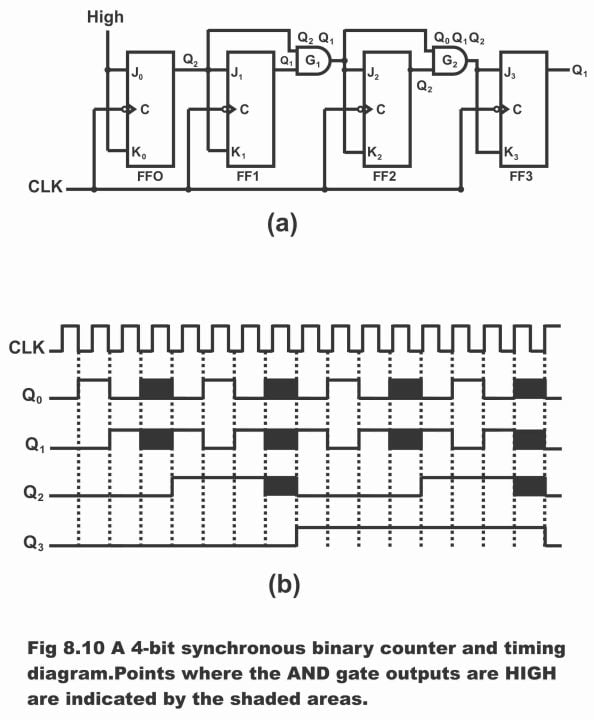
Figure 8.11-Truth table for 4-bits synchronous counter
| Number of Clock Pulses | Binary Counting Sequence | Decimal Count | |||
| Q3 | Q2 | Q1 | Q0 | ||
| 0 | 0 | 0 | 0 | 0 | 0 |
| 1 | 0 | 0 | 0 | 1 | 1 |
| 2 | 0 | 0 | 1 | 0 | 2 |
| 3 | 0 | 0 | 1 | 1 | 3 |
| 4 | 0 | 1 | 0 | 0 | 4 |
| 5 | 0 | 1 | 0 | 1 | 5 |
| 6 | 0 | 1 | 1 | 0 | 6 |
| 7 | 0 | 1 | 1 | 1 | 7 |
| 8 | 1 | 0 | 0 | 0 | 8 |
| 9 | 1 | 0 | 0 | 1 | 9 |
| 10 | 1 | 0 | 1 | 0 | 10 |
| 11 | 1 | 0 | 1 | 1 | 11 |
| 12 | 1 | 1 | 0 | 0 | 12 |
| 13 | 1 | 1 | 0 | 1 | 13 |
| 14 | 1 | 1 | 1 | 0 | 14 |
| 15 | 1 | 1 | 1 | 1 | 15 |
| 16 (recycles) | 0 | 0 | 0 | 0 | 0 |
Previous Topic: Counters in Digital Electronics: Synchronous, Asynchronous and Ripple Counter
Next Topic: Down Counters and Up-Down Counters in Digital Electronics
For electronics and programming-related projects visit my YouTube channel.
Discover more from Electronic Clinic
Subscribe to get the latest posts sent to your email.