Transistor as an Amplifier Working and Circuit Diagrams
Last Updated on April 27, 2022 by Engr. Shahzada Fahad
Table of Contents
BJT APPLICATIONS
Transistor as an Amplifier:- Bipolar junction transistors are mostly used for amplification and switching purposes. The detail is as below
BJT Appliances
Basically, a transistor can be utilized as an amplifier or as an amplifying unit. Its biggest advantage is that if a weak electrical signal is provided between its two input terminals, it magnifies the power of this weak signal. (or amplifies it), thus an amplified electrical signal can be received between the other two output terminals. This operation is called amplification. As there are just 3 terminals in a transistor, therefore it should be kept in mind that one of its terminals (called the ground terminal) is common with its input and output. (i.e. one of the three terminals of a transistor is used for input and one for output, while the third one is used as a ground and which is common for both input terminal and output terminals)
When a transistor is desired to be operated as an amplifier, it is connected with any one of three following methods.
- Common-base amplifier
- Common-emitter amplifier
- Common-collector amplifier
Above mentioned 3 circuits have been shown in figure 4.8
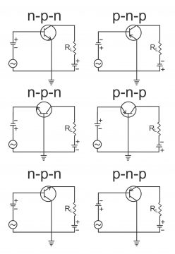
Common Base (CB) Amplifier
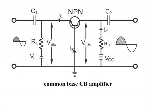
In this circuit, the transistor is fitted in such a manner that the base is common or ground both between input and output circuits (i.e. base is common both for emitter and collector on this circuit). The input signal is provided parallel to the emitter-base (EB) junction and the amplified output signal is received from the collector base (CB) junction. Since the base is common or grounded for both the signals, this circuit is also called a grounded circuit.
In diagram 4.9, a single-stage amplifier circuit with an NPN transistor has been demonstrated. When input supplies a-c signals to the emitter-base junction, the output is received from the collector-base circuit (or parallel to the load resistor). E/B junction is forward bias through VEE while C/B junction is reverse bias through VCC. Due to the E/B junction being forward biased, its impedance is low, while the impedance of the C/B junction is very high due to being reverse bias.
Circuit Operation of CB Amplifier
When the positive half of the signal combines with input:
- Forward bias is reduced, because, according to biasing law, VBE (voltages found parallel to emitter and base) are already negative with respect to ground.
- Beta current (IB)declines due to a reduction in emitter voltage.
- IE and IC also are reduced (because these two currents are nearly equal beta times of base current)
- Drop IC RC decreases with the collector voltages getting more positive
- Thus, there is an increase in output voltage VCB, which can be denoted via the following equation.
VCB= VCC– IC RC
Thus, signals’ positive half cycle amplifies on output, as has been displayed in the diagram. During the negative half-cycle, the above-mentioned process gets inversed (i.e. as forwarding bias increase, emitter voltage also increase as a result. Due to an increase in emitter voltage, emitter current and collector current also increase. With an increase in collector current, drop-in load resistor RC also increases. As the change in collector current is nearly the same as in emitter current and as the resistance of collector is far greater than emitter’s, therefore huge voltage drop occurs on load, due to which a several times the higher signal is received on output)
As positive input signals produce positive output signals, therefore, no phase reversal exists between input and output signals on such a circuit (i.e. input and output signals are of the same form and no change occurs in their phase). Due to the input and output resistance of the circuit, voltage amplification is possible instead of current gain. (which is always less than unity). The resistance of the input circuit is low, whereas the resistance of the output circuit is very high. Although changes in output and input currents are the same, there, however, exists a large ac drop parallel to the load resistor. Therefore, large changes occur in VCB (which are output voltages) due to input ac signal, by means of which voltage amplification takes place.
Characteristics of a CB Amplifier
This amplifier has the following characteristics.
- Its input resistance is very low (30-150 ohm)
- Its output resistance is very high (up to 500-kilo ohm)
- It has a current gain lesser than a unity
- It has an abysmally high voltage gain (approx. 1500)
- It has a power gain up to 30Db
- No phase reversal occurs between the input voltage and output voltage
- The circuit remains stable despite variations in temperature
Uses
In this method, as the quantity of collector current is about 5% less as compared to emitter current, that’s why it is relatively less used. These currents are mostly used on high frequencies. An important application of a common-base amplifier is the matching of a low impedance circuit with a high impedance circuit.
Common Emitter (CE) Amplifier
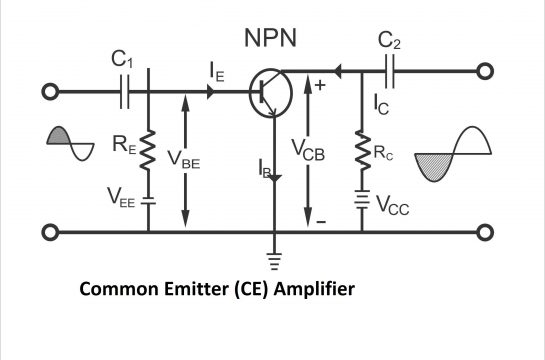
When a transistor is fitted on a circuit in such a way that the input signal is provided parallel to its base-emitter junction and output is received through the collector-emitter junction, while the transistor is kept common or grounded, it is called a common emitter circuit. It is the most popular method used for amplifying a transistor by fixing a circuit. In other words, a CE circuit is one, wherein the emitter is being grounded. The input signal is provided on the base, while the output signal is received through a collector.
In diagram (4.10) a single-stage CE amplifier circuit has been illustrated, in which an NPN transistor has been applied. Here, the base is a driven element (i.e. base current works in the capacity of input). The input signal is provided through the base-emitter circuit, whereas the output signal is received through the collector-emitter circuit. EB junction is forward biased via battery VBBand C/B junction reverse-biased through VCC (In fact, the same battery VCCcan supply dc power both to base and collector)
Now, we analyze that when ac signals are provided on a circuit’s input, what happens next.
Circuit Operation of CE Amplifier
When the signal’s half positive cycle is supplied, then
- As per biasing rule, as the transistor’s base is already positive due to being grounded, VBF
- An increase in VBE also increases the forward bias of emitter junction
- IB also goes through some (or a little) increase
- Due to an increase in IB, IC increases β times (because IC= β IB)
- There is a substantial increase in RC drop
- VCE decreases according to the following equation
VCE = VCC – IC RC
- VBF decrease in the presence of a negative signal
- Base current (IB) and collector current (IC) decrease
- Voltage drop on IC decrease
- VCE increase, resultantly output signal also increases
Thus, the negative half cycle of the signal is achieved, which means giving a negative input signal on such a circuit, leads to an amplified positive output signal (as depicted in the diagram)
Current Gain
The mutual ratio between a transistor’s output current (IC) and input current (which is IB in the situation of a common-emitter) is known as a current gain of the transistor. In other words, the ratio of collector current to a base current is called current gain and it is denoted by Ai. i.e.
Ai= IC/IB
Since the signal moves into a CE amplifier circuit via a base which causes variations in collector current, therefore a current gain of the circuit equals β. Remember that βdenotesratio of change between base current and collector current i.e.
Ai = IC/IB= β
Voltage Gain
The mutual ratio between output voltage (Vo) and input voltage (Vi) is called voltage gain and it is denoted by Aυ. i.e.
Aυ= Vo/Vi = β IB RC/ β rc IB= RC/ rc= ro/r c
As voltage gain can also be described with respect to input resistance and output resistance thus, the voltage gain of a CE amplifier circuit can also be defined as
A υ= β. output resistance/input resistance= β. ro/ rin
Entering a value of rin, which is βrc, in the above equation
A υ= β. ro /β rc= ro/ rc
Power Gain
The product of a voltage gain and current gain is equivalent to power gain i.e.
AP = Aυ Ai = β. rυ / rc
In decibel form, power gain can be written as follows
Gp= 10log10AP……..dB
Characteristics of a CE Amplifier
A CE amplifier consists of the following characteristics
- Its input resistance is low to a reasonable extent (i.e. 1k – 2k)
- Its output resistance is moderately high (i.e. 50k or above)
- Its current gain (β) is quite high (50 – 300 times)
- Its voltage gain is very high (1500 or above)
- It produces a very high-power gain (10000 times or 40dB)
- It yields phase reversal of input signal i.e. input and output signals produce at a difference of 180º from each other (or input and output signals are mutually 180ºout of phase)
Uses
Most of the transistors are of CE type because current generates very high gain with respect to voltage and power. Further, its input and output impedance characteristics are apposite for various applications. Such types of circuits are mostly used in cascade stages amplifiers.
Common Collector (CC) Amplifier
A circuit, the transistor base of which is exerted a base signal (just like a common emitter circuit) while the collector of this transistor is kept common or earthed, is called a common collector circuit.
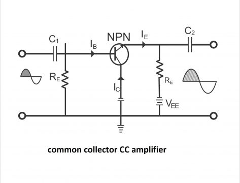
In diagram 4.11, a single-stage common amplifier circuit, in which an NPN transistor has been used, has been illustrated. The input signal is provided through the base-collector circuit and the out signal is received through the emitter-collector circuit. E/B junction has been forward biased through VEE battery whereas C/B junction reverse-biased through battery VCC. Now we study what happens in the event an AC signal is provided parallel to the input circuit.
Circuit Operation of CC Amplifier
When signals’ positive half cycle is offered, then
- Forward bias increases, because VBE are positive with respect to collector or ground.
- Base current IB increases
- Emitter current IE increase
- Drop parallel to RE increase
- Output voltage also increases due to an increase in RE drop
Consequently, we get output’s half positive cycle in an amplified state. As providing a positive signal on input also results in a positive signal on output thus, input and output signals are mutually in-phase.
Characteristics of a CC Amplifier
A CC amplifier comprises the following characteristics
- Its input impedance is high (i.e. 20k – 500k)
- Its output impedance is low (50 – 1000 ohm)
- Its current gain is high
- Voltage gain is less than unity
- Power gain ranges between 10- 20dB
- Input and output signals are mutually in-phased
Uses
CC amplifier is used for the following purposes
- for impedance matching i.e. for connecting a high output impedance circuit with a low input impedance circuit
- for circuit isolation
- Since it can pass a signal in any direction thus, it might also be used as a two-way amplifier
- for switching circuits
Comparison of CB, CE, and CC Amplifier Circuits :
Comparison of Common Base, Common Emitter, and Common Collector Circuits
In table 4.1, a comparison of Common Base, Common Emitter, and Common Collector circuits has been illustrated in a simple way.
Table 4.1
| Characteristics | Common Base | Common Emitter | Common Collector |
| Voltage Gain | Large | Very Large | Nearly Unity |
| Current Gain | ͌ 1 (α) | Large (β) | Very Large (1+ β) |
| Power Gain | Moderate | Very Large | Small |
| Input Resistance | Low | Moderate | High |
| Output Resistance | High | Moderate | Low |
| Phase Reversal | No (Zero Degree) | Yes (180 Degree) | No (Zero Degree) |
| Leakage Current | Very Small | Very Large | Very Large |
| Applications | For High-Frequency Applications | For AF Applications | For Impedance Matching |
Collector Curves and Operation Regions of Transistor
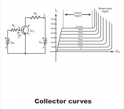
For understanding the operation regions of a transistor, it is first necessary to understand collector curves. In diagram 4.12 (a) a circuit has been presented by means of which collector curves can be formed. These curves have been exhibited in figure (b). Remember circuit comprises an NPN transistor tailored on a common emitter series.
If we change base voltages VBB and collector voltages VCC of the CE circuit shown in the figure (a) and measure collector current IC and collector-emitter voltage VCE, and draw out a curve between them on the basis of these dimensions, it is called collector curve. Different types of such curves have been illustrated in diagram (b)
When the value of VCE is zero, at that point collector-base junction (or collector diode) is not reverse biased; as a result collector current is zero. However, as soon as the value of VCE is increased initially to some extent, IC increases very swiftly and then stops. Practically, its reason is 0.7-volt reverse bias of the collector diode. The vertical part of curves closer to the origin is called the saturation region. In this region, the collector diode is slightly forward biased because here the value of VCE is less than 0.7 volt. The increasing value of VCE slightly above 0.7-volt reverses bias collector diode. In this situation, the collector current almost becomes constant.
When collector voltages are increased quite significantly, the collector diode tends to break down, due to which collector current increases very speedily (figure b). Normally, the transistor should be protected from operating in the breakdown region, as it could get wasted due to large power dissipation. For example, if the breakdown voltage value of some transistors is 40-volt, the value of VCE under normal circumstances should be less than 40 volts.
An active region of a transistor is one, where collector curves become almost horizontal or constant. In the active region, the value of collector current equals nearly 100 times the value of base current. In other words, the entire area between a saturation region and the breakdown region is an active region. (If a 2N3904 transistor is being used, changing the value of VCE from 1 volt to nearly 40 volts results in an active region). In this region, change in VCE has very little impact on IC. A change in IB is required for bringing about any change in IC.
In the diagram, the value of IB in the lowest curve is zero. This region is called a cut-off region. Due to the current leakage of the collector diode, very little collector current survives in this region. The leakage current in silicon transistors is so low, that’s why its use is ignored in the majority of applications. (Leakage current of 2N3904 transistor is only 50 nano amperes which is such an insignificant value that the lowest curve turns almost invisible)
Close attention towards the below detail /curves reflects that there are only four important parts where a transistor operates in various styles. All four regions are known as transistors’ operation regions. A brief description of these regions has been mentioned as follows:
Active Region
The center region of any collector curve which is almost horizontal is known as an active region. It is a normal operational region of some transistors. In other words, the middle region between saturation and breakdown areas is referred to as an active region. This is the most important region wherein collector current (IC) almost remains constant. Further in this region, the emitter-base diode is forward biased whereas the collector-base diode reverses biased. (In the case of the 2N3904 transistor, this region upholds if values of VCEare changed within 1 volt to 40 volts). There is no noticeable impact of a change in VCE on IC.
Breakdown Region
When the value of collector voltage increases gets too high, the collector diode tends to breakdown, as a result of a sharp increase in collector current. Region of a transistor at which the collector diode breakdowns upon an increase in collector voltage, is called the breakdown region (in the case of the 2N3904 transistor, when collector voltage increases past 40 volts, its breakdown region starts). As collector current tends to increase very quickly in the region, therefore, the transistor is never used in this region; otherwise, it could get ineffective or destroyed completely. Remember, this region is also called the reverse active region because here emitter-base diodes are reverse biased while collector base diodes are forward biased (i.e. completely opposed to the active region)
Saturation Region
In this region, both emitter-base diode and collector base diode is forward biased. When the value of VCE is enhanced from zero to approx. 1 volt, the starting point of collector curve is of slightly sloped type or approx. vertical near the origin. The region, where the initial part of the curve is sloped type, is called the saturation region. However, remember that in certain transistors, e.g. 2N3904, the horizontal region of the curve starts well before (i.e. 0.3 volts) increasing the value of VCE to 1 volt.
Cut-off Region
Transistors’ operation region, where the first or lowest curve is formed when the value of base current IB is zero, is called a cut-off region. In this region, both emitter-base diode and collector base diode is reverse biased. In diagram (b) collector curves have been drawn in the form of different base currents (e.g. first curve is drawn at zero base current value, 2nd curve at 10µAbase current, and 3rd collector curve is 20µA base current). The lowest one amongst the curves is formed when the value of the base current is zero. This is a cut-off region as only a small collector current prevails in this region (due to the leakage current in the collector diode) which is called a cut-off current. Due to this minor value of collector current, it is difficult to draw a collector curve. For clarification of transistors operation in the region, the curve is drawn extremely cautiously. The operational region of a transistor where this curve is drawn is called a cut-off region.
Bipolar Junction Transistor (BJT) As A Switch
As no bias voltages are applied on a transistor’s base in digital logistics circuits, the transistor operates only in saturation and cut-off regions in these circuits. Due to this, the low or high output voltage can be received. Therefore, BJT is most massively used for transistors’ switching purposes. Remember when a transistor is used for this objective, input waveforms that are provided to it, keep on changing between low and high voltages (i.e. 0 volts to +5V). The circuit which is basically used for switching purposes is called an inverter. An NPN transistor inverter or switch has been illustrated in diagram 4.13
It is evident from the diagram that transistor CE has been mounted on a series sequence; however, no bias voltages (dc voltages) have been supplied on its base. Rather a square type input waveform has been provided directly to the base via fitting a transistor RB on-base series, which functions as inverter input. It is clear from a circuit that the value of both VCC and input’s high level is +5V, whereas voltages (VCE) received between collector and emitter are output voltages.
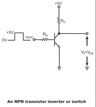
When an inverter’s input is high (+5V) base-emitter junction is forward biased and current flows towards the base via RB. Normally, those values of RB and RC are chosen on which value of base current (IB) is such that a transistor can be saturated (i.e. the value could operate the transistor in a saturation region with its output characteristics). In figure 4.14, a load line has been depicted, which has been drawn on a set of CE output characteristics. In the load line, the point where saturation occurs has been elaborated. According to this point, the VCE value, which is called (SAT), is almost zero volts. The current at saturation point is called (SAT) IC and its value are equivalent to VCC/ RC.
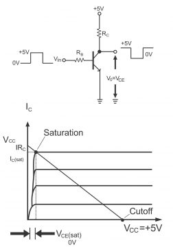
When the transistor saturates, it is called (on). In such a situation (i.e. when the inverter’s input is high or +5V), the output of the transistor is low (i.e. zero volts). On the contrary, when the transistor’s input is low, its base-emitter junction no longer remains forward biased, due to which neither base current nor collector current occurs. Therefore, there are no voltage drops parallel to RC. Consequently, the transistor’s output becomes high (+5V) due to its low input. Thus, under such a situation, the transistor remains in the cut-off region of its characteristics and it is called (off). As high output produces as a result of low input, that’s why the circuit is called an inverter.
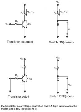
From the above discussion, it has become clear that as a transistor’s (on) and (off) conditions resemble (open) and (close) conditions of a switch fitted between emitter and collector, therefore, a transistor inverter is often known as a transistor switch. When the transistor is on or saturated, the transistor’s voltage value found between emitter and collector equals zero just like the voltage value parallel to close or on the switch, while the current value is maximum (i.e. VCC/ RC). Inversely, when the transistor is on or off, the value of current flowing from collector to emitter is zero just like an open switch, whereas the voltage value is maximum under such circumstances. Switch open or close through input voltage (i.e. open/ close of the switch depends on the value of input voltage). Switch close in situations of high voltage, and open as a result of low input (figure 4.15). In diagram 4.16, an ideal switching action of a transistor has been illustrated.
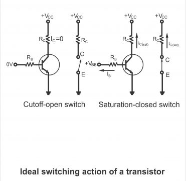
On digital circuits, a transistor is not practically operated on any point other than its saturation and cut-off region, therefore, the transistor is just used as a common switch on such circuits. In various applications like switches, the emitter is connected with some other circuit or voltage source instead of being grounded. For instance, if an emitter instead of being grounded, is connected with -5V on a basic inverter circuit, the output will clearly switch between +5V and -5V instead of +5V and zero volts. Thus, a digital circuit is also called a switching circuit, because the transistor operates as a switch between two extreme ends of its load lines. Remember, these extreme ends or points are saturation and cut-off regions and such circuits are occasionally called Two-State- Circuits.
For electronics and programming-related projects visit my YouTube channel.
Previous article: Bipolar Junction Transistor and Next article: Field-Effect Transistors
Discover more from Electronic Clinic
Subscribe to get the latest posts sent to your email.
