TTL Circuit: Transistor -Transistor Logic Circuit Operation
Last Updated on October 25, 2022 by Engr. Shahzada Fahad
Table of Contents
Transistor -Transistor Logic Circuit – TTL Circuit
Transistor-transistor logic (TTL) is the most popular and widely used family of digital devices, which was introduced by Texas Instruments in 1964. Transistor – transistor logic circuit is a logic circuit, in which instead of fitting diodes on inputs (as is done in DTL circuits), multi- emitter transistor (a transistor which has two or more than two emitters, is known as multi- emitter transistor) has been mounted. In other words, a logic circuit, the input, and output of which consists on just transistors, is called a TTL circuit. We may also shortly call TTL as TL. It is a saturated logic. This circuit has vastly been in use since 1970 due to its high speed, better fan–in and fan–out, simple use, and an easy interfacing features (a process in which the output of two or more than two devices is interconnected with the input of another device so that combined together they could work according to our will and needs, is called interfacing).
The greatest advantage of a TTL circuit is that a multi-emitter transistor is used on its input and the number of transistors emitters is equal to the circuits’ fan–in. Therefore, instead of using a number of diodes on a DTL circuit input, only one multi-emitter transistor is mounted on TTL circuit, hence TTL occupies far less space as compared to a DTL circuit. As a multi-emitter transistor is quite smaller in size as compared to a diode, therefore the size of the wafer (on which this transistor is mounted) becomes larger, which is thus, brought into use in a far better way. Moreover, as a result of a smaller multi-emitter transistor area as compared to a diode, low capacitance generates on substrate. As a result of this, the circuit speed increases due to a reduction in the rising and falling times of the circuit. Remember that this family comprises (SSI circuit series) simple gates and flip–flops, (MSI circuit series) various shift registers being used in computers (LSI series) microprocessor bit-slice chips, and a very broad selection of circuit modules. In other words, simple gates and flip–flops, various shift registers being used in computers, and microprocessors slice chip bits are manufactured on lines of the TTL family.
Performance Characteristics of a TTL
The transistor-transistor logic (TTL) type integrated circuits offer excellent performance due to the following characteristics:
- Their speed is very high
- It has a low price
- Their Fan-in and fan – out is quite good
- Their interfacing with other digital circuits is quite easy
- Their noise margin is high
Basic TTL NAND Gate Circuit
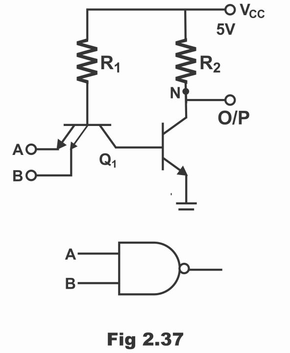
The basic NAND circuit of a TTL family has been shown in figure 2.73. However, apart from the NAND gate, other configurations like NOR, OR, AND have also been included in this series.
Circuit Operation
The explanation of a TTL NAND gate circuit is as follows:
When Both Inputs Are High
If both inputs A and B are high (logic 1), the emitter–base (E/B) junction of Q1 transistor becomes reverse biased, due to which no emitter current passes through the emitter. Thus, in such a situation, Q1 turns OFF. However, its collector–base (C/B) junction is forward-biased, due to which transistor’s base Q2 receives base current via R1 from +VCC. As a result, transistor Q2, fully turns ON (i.e. Q2 gets saturated). When Q2 is ON, zero voltage are received on point N. Therefore, in case both inputs are high, a low output is received (i.e. output logic is at zero)
When Both Inputs or Either Input is low
When both or any one of the two inputs is low (i.e. it is at logic zero), the associated emitter–base (E / B) junction (or the junction with low input) becomes forward-biased. Thus, transistor Q1 turns fully ON. (Remember that value of R1 is selected in such a manner that Q1 could fully get ON). In case Q1 is saturated or ON, the voltage at point M becomes zero. Resultantly, the base current of transistor Q2 also becomes zero. As a result of the zero-base current of Q2, this transistor turns OFF. Thus, high voltage equal to +VCC on point N are received. In other words, high output results on point N (that’s output is at logic 1).
Major Types of Output Circuits for TTL Gates
A TTL gate has the following two important types with respect to output circuit
- TTL NAND Gate Output with Totem Pole Output
- TTL NAND Gate with Open collector Output
Explanation of the aforementioned two types is as under:
TTL with Totem Pole output
The basic circuit of a TTL (which has been shown in figure 2.37) practically does not come into usage. Normally a slight modification is carried out in this circuit by adding an output stage along with it (i.e. an additional stage consisting of Q3, D and Q4 is included along with output of basic TTL circuit) which has been illustrated in figure 2.38. This additional output stage is generally referred to as a totem pole stage. The basic TTL circuit with which a totem pole stage is added, is called totem pole output TTL circuit, which is briefly known as totem pole output. It is worth mentioning here that output transistors Q3 and Q4 develop totem pole connections, which mean that one transistor is in series of the other.
In simple words, totem pole is a type of output, which depends on the designing of the circuit, which type of output would you like to take.
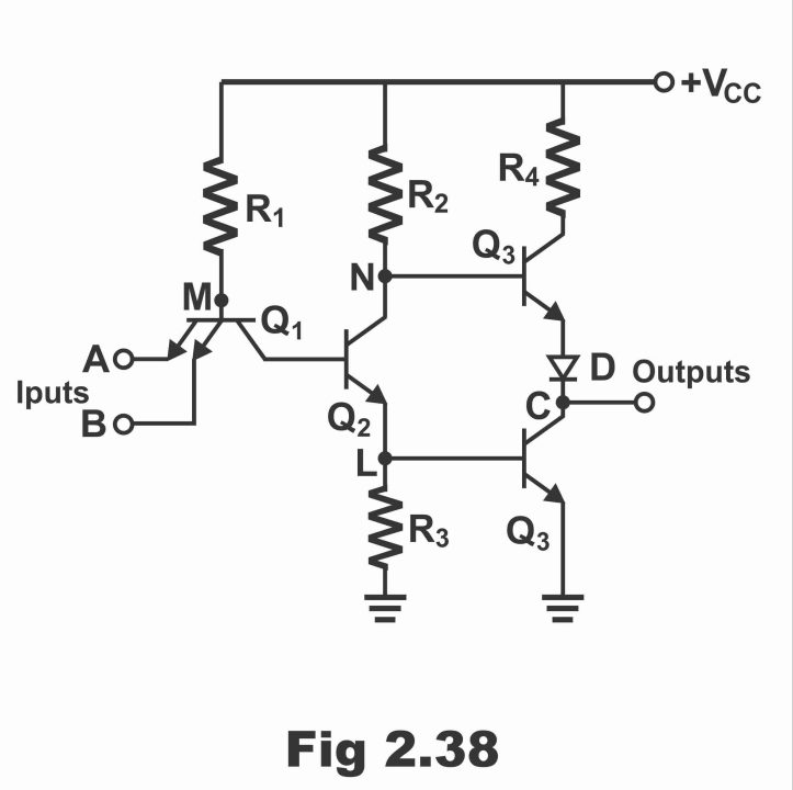
Circuit Operation
The explanation of the totem pole circuit’s operation is as under:
When the input is high
When the input is high, in such a situation positive voltage is received on both input terminals (that’s logic 1 state occurs on both the terminals). Thus, emitter-base of transistor Q1 (E/ B) junction becomes reverse biased, due to which there is no emitter current at all (that’s the flow of current through the emitter is zero) and Q1 becomes OFF. As the collector–base (C /B) junction of Q1 is forward-biased, thus current flows from VCC through R1 toward the base of Q2. Thus, Q2 turns ON. As a result, the potential of point N gets so minimum, that transistor Q3 turns OFF (because the signal is received on Q3 base via point N). As voltage drop occurs exactly at that time parallel to R3, therefore Q4 gets ON. Now when Q4 is ON, the potential of its collector (i.e. potential of point C) becomes almost equal to its emitter’s potential, resultantly a low output is received (that’s output is at logic state)
In short, when input is high (or on logic 1) then Q1 remains OFF, Q2 ON, Q3 OFF and Q4 is ON, as a result of which output tends to remain low.
When Input is low
When any one of either inputs or both inputs are low (or at logic level 0), in such a situation Q1 remains ON, and potential of its collector (i.e. potential of point M) declines. Due to which Q2 becomes OFF. As a result of OFF Q2, potential of both its emitter as well as Q4 base becomes zero (that’s Q2’s emitter which provides signals on Q4 base via point L) and Q4 base gets grounded, thus Q4 also turns OFF. As the potential of N equals VCC’s potential, therefore Q3, turns ON. The potential of point C is obtained by subtracting the total drop occurring in R4, Q3 and D from VCC. As the value of these drops is not very high, therefore practically a high output is received (that’s the receivable output is at logic 1)
In order to easily understand afore – mentioned operation of the circuit, it must be kept in mind that even numbered (i.e. 2, 4) transistors are ON, the odd numbered (i.e. 1,3) transistors remain OFF. And when odd numbers transistors are ON, even numbers transistors are OFF.
In figure 2.38, the function of diode D mounted between Q3 and Q4 is to thwart Q3 and Q4 from turning ON simultaneously. If both these transistors turn ON at a time, they will offer very little impedance on supply, by means of which maximum current will flow towards the output, which will resultantly cause to generate too much noise on output. It must also be inculcated that operating speed and output current capability of this circuit enhances as a result of adding a pair of totem pole transistor.
Advantages of Totem Pole Output Circuit
Standard totem pole output, TTL family consists on following characteristics and advantages
- Their operating speed is quite high as compared to DTL due to a low delay time
- Noise immunity is low (0.4V)
- Average propagation delay per gate is 10 nano seconds (ns)
- Average power dissipation is 10mW
- Its maximum fan – out is 10, which means that an output can drive 10 other TTL inputs
- It has a fan – in of 6
- Its inter – facing with other digital circuits is easy.
- The multi – emitter transistors applied in it occupy relatively small space as compared to diodes
- This family is relatively cheap and readily available in the market in large quantity
- Its application is simple and easy
- Totem pole transistors offer very low output impedance in binary 1 (high) state
- TTL devices are compatible (i.e. output of one TTL device can be provide as input to other TTL device. In such a situation, first device is called driver whereas the second one as load)
- They can operate quite efficiently between 0 – 70°C
TTL Gate with Open Collector output
Some of the TTL devices comprise open collector output instead of a totem pole output. It means that only the bottom transistor (i.e. Q4) of the totem pole pair is applied in them. Thus, a totem pole output TTL gate, in which only the bottom transistor of the totem pole output’s additional stage is used and output is received from such a transistor’s open collector, is known as open-collector output TTL gate. In figure 2.39, an open collector output TTL NAND gate (which consists of two inputs) has been illustrated. A multi–emitter transistor Q1 has been used in it, whereas the output is received via an open collector of transistor Q4. Outputs of various open collector gates can be inter-connected via wires, see figure. As collector of Q4 is open, therefore an outer resistor is mounted on output in order to get a reasonable output from this gate, which is known as pull – up resistor, as has been manifested via figure (b). This pull–up resistor provides a high voltage level once transistor resistor Q4 is OFF. In figure (c), three TTL devices have been shown inter–connected with pull – up resistor. It must be remembered that in some of the systems, outputs of as many as 16 open collector devices is linked with pull – up resistor, total output is thus, received.

Circuit Operation
- When both inputs A and B are high (i.e. logic 1), the emitter–base (E/B) junction of Q1 reverse biases, by means of which it becomes OFF. However, collector – base (C/B) junction of Q1 becomes forward-biased, thus Q2 turns ON as a result of signal voltage received on Q2 ‘s base. As Q2’s emitter is connected to Q4 base, thus Q4 also turns ON or saturates as a result of Q2 being in ON state. As a result, a low output is received on Y (or voltage level become zero at Y). Thus, when both the inputs are high, Q1 becomes OFF, Q2 ON and Q4 also turns ON, due to which becomes low (or logic zero).
- When both inputs or any one of the inputs is low, in such a situation Q1 becomes ON or saturates and its collector potential also reduces, owing to which Q2 becomes OFF (because Q1 collector provides signal on Q2 base). As a result of Q2 being in OFF state, Q4 also turns OFF and output point, reaches +5V due to pull – up resistor (i.e. output becomes high)
Thus, when both inputs or any one of the two inputs is low, Q1 is ON, Q2 OFF and Q4 is OFF, due to which output becomes high. It should be remembered that this condition also applies to the working operation of an AND gate.
The greatest flaw of an open collector gate is that its switching speed is extremely low, due to the value of pull – up resistor being few kilo ohm (1 kilo ohm to approx. 10 kilo ohm). Because when this value of pull – up resistor is multiplied by the stray output complement, time constant RC relatively increases. Remember, a higher pull–up resistor value means higher time constant and high time constant implies a very low switching speed. This happens due to the charging of input complements via the pull–up resistor. When output varies from low to high, slow switching speed of open collector TTL device becomes even more defective. Open collector gate is mainly used for illuminating lamps, relay, LEDs or for driving a diode.
Previous Topic: Selection of Logic Gates or Digital Integrated Circuits
Next Topic: Half adder and Full adder with Equations in Digital Electronics
For electronics and programming-related projects visit my YouTube channel.
Discover more from Electronic Clinic
Subscribe to get the latest posts sent to your email.

