Half adder and Full adder with Equations in Digital Electronics
Last Updated on October 25, 2022 by Engr. Shahzada Fahad
Table of Contents
Binary Addition
Half adder and Full adder with Equations in Digital Electronics- Binary arithmetic is used in digital computers, calculators and several other digital systems of different types (as computer circuits process binary numbers instead of digital numbers), therefore engineers and workers working with digital appliances and circuits should be fully conversant with binary addition or binary subtraction in order to comprehend the operation of digital systems. As binary addition occupies a pivotal place for understanding binary subtraction, division and multiplication, therefore it is essential to have adequate knowledge about binary addition.
We are aware of decimal addition process of calculation under a decimal system, in which digits of tens, hundreds and thousands are transferred to the next left column in the shape of carry at the time of adding decimal numbers. In this way, the process of decimal calculation is somewhat difficult and lengthy.
As binary system comprises two digits (i.e. 0 and 1), therefore addition in binary system is relatively easy one as compared to the decimal system. The following four basic rules should be kept in mind while calculating binary numbers:
0+0=0 … sum of 0 with a carry of 0
0+1=1 … sum of 1 with a carry of 0
1+0=1 … sum of 1 with a carry of 0
1+1=10 … sum of zero with a carry of 1
Afore – mentioned principles can also easily be understood via binary addition tables shown in figure 3.1 (a)
Figure 3.1 – (a). Binary addition tables (b). Sample binary addition problems
The first three problems in situation of addition through decimal are easy, however third or fourth problem is relatively complicated, because the answer of 1+1 in decimal is 2. Remember that 2 is represented by 10 in binary (here 0 is total while 1 is carry). That’s why in the fourth problem, 1+1 is reflected by 0 instead of 2 (i.e. 1+1 = 0), whereas sum total 1 in this method is carry, which is added to next stage or next left side digit or next column.
In figure (b) some examples of addition of binary numbers have been presented and with each example, addition of decimal numbers has also been elucidated, so that binary can be learnt easily. In the first example, binary 10 has been added to binary 101, the answer of which is binary 111 (remember that binary 101 equals to decimal 5 whereas binary 10 equals to decimal 2, whereas we get answer 7 by jointly adding decimal 5 and 2, which is equivalent to binary 111). This example or problem is very simple one.
In figure (b), binary 11 is added to binary 1010 in the second example. By carefully looking at this example, one can understand that by adding binary 1 with binary 1 in the second column, we get 1 carry which transfers to the third column or next left column, thus we get answer as 1101 (or in decimal the answer will be 13)
In figure (b), the third example displayed is a relatively somewhat difficult one, because here carry is transferred to the next columns two time. In this example, binary 11010 and binary 1100 have been added together. Therefore, in case of two carriers, the answer in terms of binary numbers is 100110 (or in case of digital numbers 38).
Adder
A logic circuit, which is used to add two binary numbers, is known as adder. Adder is not only being used in computers, its application in other digital systems of numerous types, which process numerical data, is also quite important. Adders have following two types:
- Half – adder
- Full – adder
Half Adders
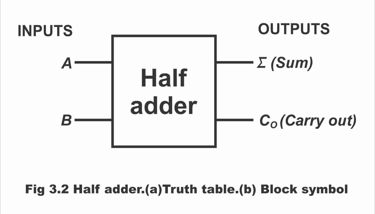
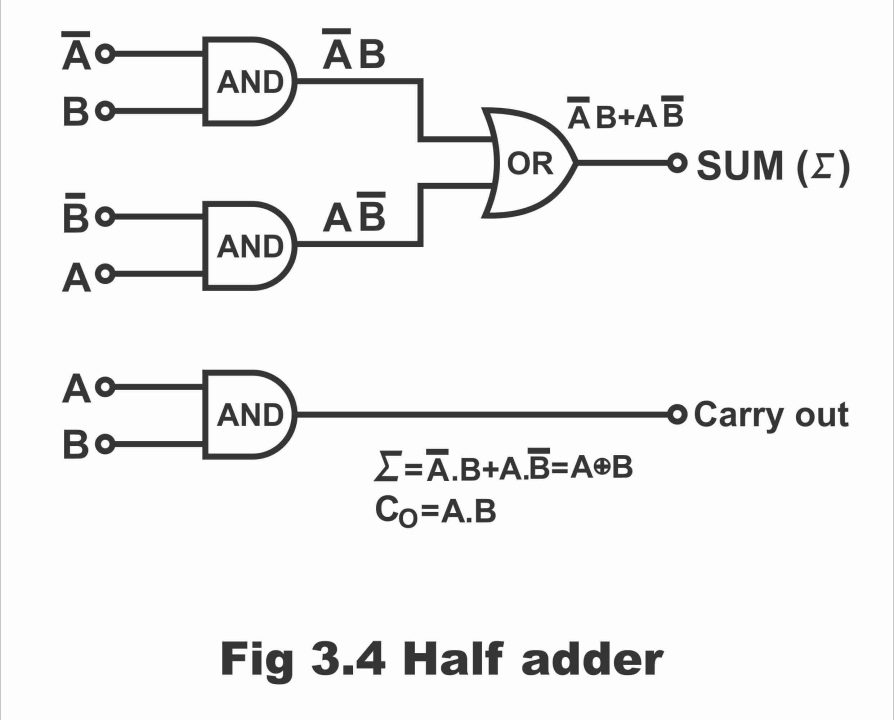
A logic circuit or device which can produce 2 – bit output data according to the principles of binary addition consisting sum (Ʃ) and carry output (Co) by means of simultaneously adding two bits, is known as a half adder. In other words, a logic circuit, which consists of two inputs (A & B) and two outputs (Ʃ & Co), is known as half adder. Half adder can also be defined as a logic circuit, which performs operations according to four basic principles of binary addition, is called half adder. Or a circuit, which provides sum and carry output for A and B inputs, is called a half adder, it must be remembered that half adder cannot control or handle input carriers or Cin.
The truth table of a half adder can easily be prepared through rules of binary addition.
If the inputs of a half – adder consists of two bits A & B, and output is represented by a sum total sigma (Ʃ), and (in case there is any) carry by Co (carry out or carry output), in such a situation a truth table as per figure 3.2 (a) is being obtained. The first two columns of this truth table denote inputs A and B, whereas the third column with a Ʃ sign on it, is the addition column. The fourth column in the table on which Co has been written, is carry column. In figure b, block – shaped symbol of a half adder has been shown, its shape is like a squared (four – cornered) block, which consists of two inputs A & B and two outputs Ʃ and Co.
Figure 3.2 – Half adder (a). truth table (b). block symbol
Operation
The operation of a half adder can easily be understood with the help of a truth table shown in figure (a). After studying the truth table of half – adder, it becomes clear that according to the four rules of binary addition (which have been mentioned above), when
- When both inputs A and B are zero or low, a zero value results from half – adder, which is evident from the addition column of the truth table with a Ʃ symbol above it. In such a situation, the value of carry is zero as well.
- When the value of input A is binary 1 and value of input B is binary 0, then the value of Ʃ is binary 1 on half adder’s output, whereas value of Co is binary 0, which denotes that binary sum or total of binary inputs 1 and 0 is 1 i.e. (1+0=1). However, the binary value of Co tends to be 0 due to binary inputs total being less than 2.
- When the value of input B is binary 1 whereas the value of input A is binary 0, value of Ʃ on half – adder ‘s output will be binary 1 and that of Co will be 0 (just like above mentioned situation)
- When both input A and B are binary 1, in such a situation, sum (Ʃ) value on output will be binary 0, whereas value of carry out (Co) becomes binary 1, that’s why 2 is represented by 10 in binary.
If the truth table of half – adder is cautiously analyzed, it becomes evident that Co column is exactly similar to the truth table of a AND gate (because binary 1 output is received from AND gate when both of the gates’ inputs are binary 1) and sum (Ʃ) column is analogous to the truth table of XOR gate (because output of XOR gate is binary 1 when both of its inputs are exactly opposite or inverted i.e. value of one input is 0 while that of the other is 1. Thus, a half – adder can be manufactured through the application of two – inputs AND gate and two – inputs XOR gate, as can be seen via figure 3.3
Figure 3.3 – half logic diagram

As the function of carry out (Co) is performed by two – inputs AND gate and sum function by 2 – inputs XOR gate, therefore Boolean expressions of both gates are as under:
- B = Co … AND Gate
AꚛB = Ʃ … XOR Gate
Remember that in order to perform sum function, two AND gates and an OR gate can also be used instead of a XOR gate. In such a situation, Boolean expression will be as follows:
Ʃ = A. B+A.B
In figure 3.4, a two – input AND gate for sum (Ʃ) function with a two – input OR gate circuit and an AND gate for carrying out Co function, have been shown.
Figure 3.4 – Half adder
In general, input functions A and B are readily available, however if it is not possible, then inverters have to be used in order to produce A and B signals from inputs A and B. As can be seen in the figure 3.5
Figure 3.5 – logic gate half – adder

It must be inculcated that as this circuit does not accept “carry” received from previous additions, therefore this circuit is called half – adder.
Full – adder
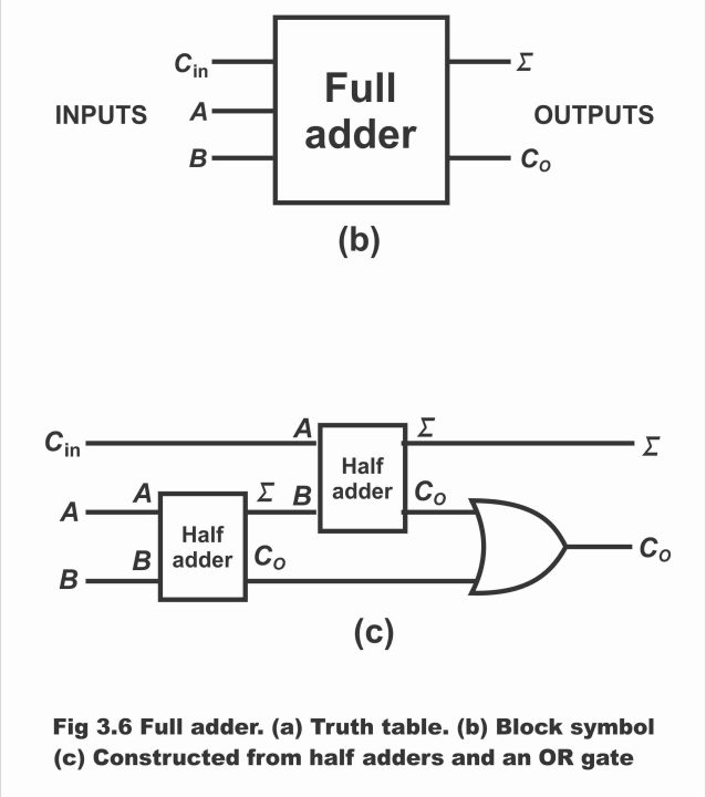
- A logic circuit which can add three bits simultaneously, is known as a full -adder
- A full – adder is a logic circuit consisting of three inputs and two outputs which can add 3 bits or digits simultaneously and provides sum and carry output
- A logic circuit which along with a carry input resulting from previous additions accepts 3 inputs and produce a sum output and a carry output, is called full – adder
Remember that basic difference between a full adder and a half adder is that a full adder accepts input carry whereas half adder does not accept input carry (i.e. in situation of a full adder, bits A and B which are required to be added, arrive from two registers whereas third input come as a carry of previous additions. Whereas contrary to this, handling or controlling previous carry feature does not exist in a half – adder.
In figure 3.6 (a) truth table of a full adder and in figure (b) its block symbol whereas in figure (c) construction of full adder comprising sum of two half adders and an OR has been illustrated. It should be kept in mind that a full adder must be used where inclusion of an additional carry input may be possible.
In figure b, it is clear from the block diagram of a full adder that it comprises three inputs i.e. Cin, A and B and we get two outputs Ʃ and Co by means of adding these three inputs.
Figure 3.6- full adder a. truth table b. block symbol c. constructed from half adders and OR gate
Operation & Working
A full adder can be constructed via the sum of two half adders and an OR gate, as has been shown via figure c. The truth table of a full adder as has been shown in the figure (a) reflects its entire possible input and output operations, explanation of which is as follows:
- When values of three inputs A, B and Cin is binary 0 (i.e. when all the three inputs are low) sum of these three inputs is 0 (that’s 0 + 0+ 0 = 0) and binary value of carry is also 0.
- When any one of three input is high (binary 1), (i.e. 1+0+0 or 0+1+0 or 0+0+1) sum is 1 or high. However, in such a situation, carry becomes low (or binary 0)
- When any two of the three inputs are high or binary 1, (i.e. 1+1+0 or 1+0+1 or 0+1+1) then sum = 0 and carry = 1 is obtained (i.e. in such a case, Ʃ value is binary 0 whereas Co value is binary 1)
- When all three inputs are simultaneously high (i.e. 1+1+1) then sum and carry both are also high or values of both sum and carry become binary 1 simultaneously.
1+1 +1
10+1 =11
This point can also easily be understood via figure 3.7 a or b. Remember that there is no difference between these two figures except that on every H.A output side, only places of Ʃ and Co have been inter- changed (i.e. in figure (a), Ʃ is on top whereas in the figure (b), Ʃ is on bottom side. Similarly, in figure (b) Co is on top side whereas in figure (b), it is towards the bottom end.
Figure 3.7

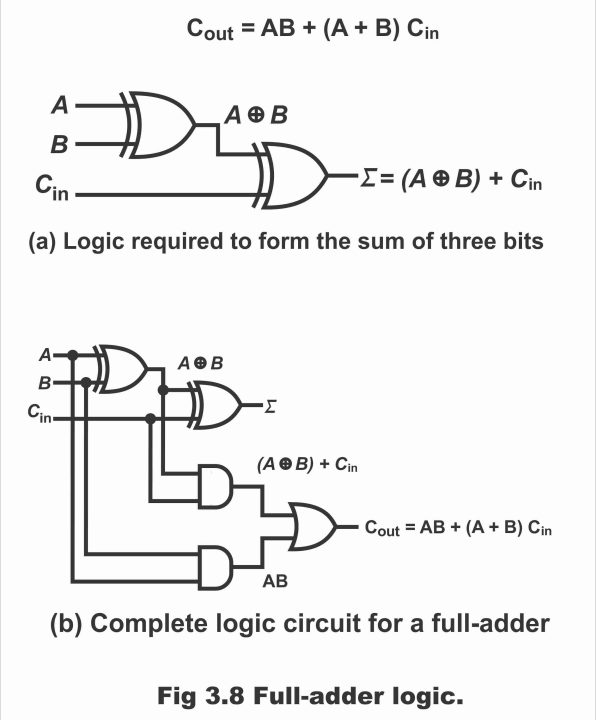
We know that a full adder adds up two inputs and an input carry. Regarding half – adder, we know that sum of inputs A and B is the exclusive OR (XOR) of both these variables i.e. AꚛB. When input carry (Cin) is added to input bits, due to an exclusive ORed operation occurring with AꚛB, we get the following sum output equation
Ʃ = (Aꚛ B) ꚛCin
It means that two exclusive OR (XOR) gates can be applied in order to perform the sum function in a full adder. The first gate operates as AꚛB whereas the second gate comprises XOR gate’s output and input carry can operate these inputs. This has been illustrated in figure 3.8 (a).
Output carry becomes 1 when both inputs of first XOR gate are 1 or when both inputs of the other XOR gate are 1. This has been elucidated via a truth table of the full adder. Thus, full adder output carry produces by means of ANDed inputs A to B and AꚛB with Cin. Both these terms then become ORed via OR gate as has been illustrated via following equation and also by figure 3.8 b. As a result of completion of this operation and combining this operation with sum logic, a full adder circuit is constructed. This has been shown in figure (b) which consists of a sum of two half adders.
Cout = AB + (AꚛB) Cin
Figure (a) – logic required to form the sum of three bits
Figure (b) – complete logic circuit for a full – adder
Figure 3.8 – full – adder logic
In figure 3.9 (a), a full – adder circuit has been represented in a simpler manner. This circuit has been fabricated on the basis of two – half adders.

Exactly below this circuit, a full – adder logic circuit has been displayed in figure b, the construction of which is relatively easy. This circuits consists of two XOR and NAND gates. Remember that this circuit also resembles to the one shown in figure (a) (that’s both circuits are used for same goals) except that in figure (b), AND and OR gates have been replaced with NAND gates. A NAND gate is a universal gate, because any digital system can be formulated through its application. For explanation, see figure 3.10 in which NOT, AND and OR gates have been illustrated with the help of NAND gates.
Figure 3.10 – implementation of NOT, AND and OR by NAND gates

It must be remembered that several circuits like half -adders and full – adders are a part of microprocessor’s arithmetic logic unit (ALU) which is used to add binary numbers in a micro-computer system consisting of 8, 16 or 32 bits. The ALU of microprocessor can also perform the function of subtraction by means of utilizing such half and full – adder circuits (in the coming pages of this chapter, you will be able to read about binary subtraction through application of adders). Half adders and full – adders are simple circuits, however complex, complicated and lengthy addition are possible through its different combinations.
Boolean Equations of Full -Adder
We know that a full – adder is constructed via a combination of two half – adders and an OR gate and this is the simplest method for the construction of a full – adder, as can be seen via figure 3.6 ©. In such a situation, Boolean equation of a full – adder is as follows:
Aꚛ Bꚛ Cout = Ʃ … (1)
A.B +Cin (AꚛB) = Co … (2)
With the help of full – adder’s truth table (which has been shown in the figure 3.6 a), the above two equations of sum or S and carry out or Co, can be derived as follows through the application of a De Morgan Theorem.
S= Ci A B + Ci A B + Ci A B + Ci A.B
Taking common
= Ci (AB + AB) + Ci (AB + AB)
Note that (AB + AB) = (AB + AB)
S = Ci (AB + AB) +Ci (AB +AB)
Let AB + AB = AꚛB Then
S= Ci (AꚛB) + Ci (AꚛB)
= Ci ꚛ(AꚛB)
Or
Ʃ = AꚛBꚛCi … (3)
Where S= Ʃ and Ci = C
And Co = Ci AB + Ci AB +Ci AB +Ci AB
By arranging the equation
= Ci AB+ Ci AB+ Ci AB + Ci AB
Taking common
= AB (Ci Ci) + Ci (AB +AB)
=AB + Ci (AB+AB)
Co- AB + Ci (AꚛB) … (4)
In figure 3.11, full – adders have explained with the help of XOR and half – adder circuits. For each digit, any binary number can be added by means of using any one circuit out of these circuits.
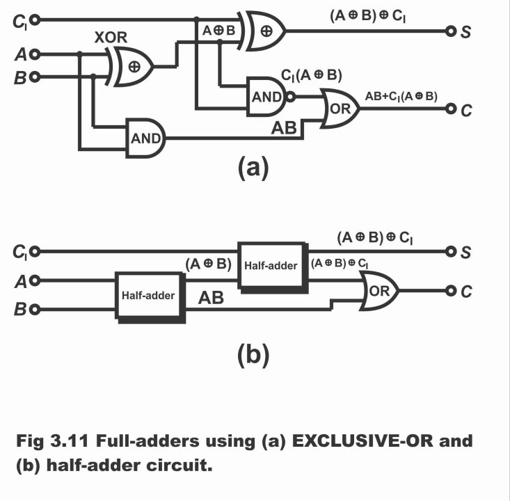
Figure – full – adders using (a) exclusive – OR and (b). half adder circuits
Previous Topic: TTL Circuit: Transistor-Transistor Logic Circuit Operation
Next Topic: Half subtractor and Full subtractor with Equations in Digital Electronics
For electronics and programming-related projects visit my YouTube channel.
Discover more from Electronic Clinic
Subscribe to get the latest posts sent to your email.