Types of Semiconductors in Electronics
Last Updated on March 22, 2022 by Engr. Shahzada Fahad
Table of Contents
Description:
Types of Semiconductors in Electronics- in this article, we will discuss different types of semiconductors in very detail.
Types of Semiconductors
Semiconductors are of the following types
- Intrinsic or Pure types of Semiconductors
- Extrinsic or Impure types of Semiconductors
There are further two types of extrinsic semiconductors.
- N-Type Extrinsic Semiconductors
- P-Type Extrinsic Semiconductors
Intrinsic types of Semiconductors
Intrinsic type semiconductor is one which is made from a semiconductor material in an extremely pure form; it does not have amalgamation of any other material.
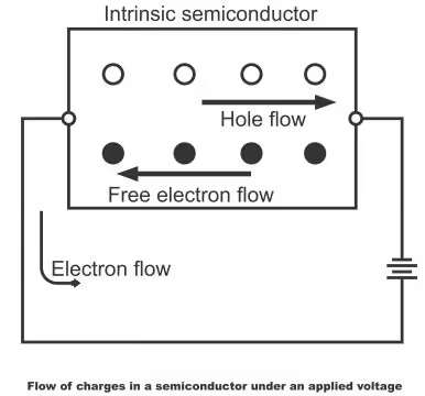
For example, a silicon crystal is called intrinsic semiconductor, when each of its atom is of silicon type. Pure germanium and pure silicon, the energy gaps of which are 0.72 eV and 1.1eV respectively, are common examples of intrinsic tpes of semiconductors. Their energy gap is so small that even at normal temperature, several electrons (through absorbing adequate energy) crossing or jumping this small energy gap, move to conduction band from valence band, due to which a positively charged hole is produced in the valence band (as shown in the figure 1.32). Semiconductor is supplied an electric field at 0⁰K temperature, conduction electrons start moving towards anode while and the holes found in cathode, start moving towards cathode. Thus, due to the mutual movement of electrons and holes in opposite directions, semiconductor current is produced in conduction and valence bands (or the flow of semiconductor current starts). Electron current come into effect due to the movement of electrons in conduction band, whereas hole current as a result of jumping of one atom to other. Therefore, an intrinsic semiconductor can also be defined as a semiconductor, in which the number of conduction electrons and holes is equal. The different forms of an intrinsic types of semiconductors have been explained below:

At Absolute Zero Temperature
An intrinsic silicon crystal has been displayed on metal end surfaces in figure 1.33 (a). An electric field is developed on middle of crystal ends through supplying an external voltage source to crystal ends. Whether current passes through crystals or not, depends on the value of temperature. If the ambient temperature is at absolute zero, then a valence orbit of every silicon atom consists of 8 electrons, as these valence electrons are so strongly combined together due to covalent bonds, that at absolute zero, these cannot be isolated from its atom. Therefore, irrespective of an applied voltage, silicon crystal functions as an insulator, because there are no free electrons in it for producing current.
At Above Absolute Zero
Atoms start vibrating as soon as temperature increases from absolute zero (that’s vibration or convulsion produces depending upon the value of temperature). As a result of this, valence electron moves from valence to conduction band through availing suitable energy. As some free electrons still exist, i.e. some free electrons can be obtained via raising temperature a little, therefore, a very small stint of current flow through the crystal, i.e. a very small stint of current generates in crystal.
With an increase in temperature, current level also increases. At room temperature (25⁰C or 77⁰F) magnitude of current passing through the crystal is very low compared to the current passing from the conductor. Therefore, this silicon crystal is called semiconductor.
![]()
A part of silicon crystal has been shown in diagram 1.33 (a). Suppose a hole and a free electron is produced through thermal energy. Free electrons continue to remain in a very big orbit. Through the application of an external electric source, free electron moves rightward. For this rightward movement, it moves from one large orbit to a second large orbit and from second to a third large orbit. In this way, free-electron takes part in the cumulative flow of electrons within a silicon crystal. Thus, we can inculcate the concept of a steady stream of free electrons from a negative source terminal to a positive source terminal (as shown in figure a)
Hole Flow
Only free electrons exist in a conductor with no holes in it at all. (Hence, charges flowing in a conductor just have free electrons i.e. charges flow in a conductor only as a result of free electrons and remember that the rate of flow of a charge is called current). In a semiconductor, both electrons and holes do exist. When external voltages are provided to a semiconductor, the electrons and holes existing in it, move in opposite directions (shown in figure 1.34). Due to which, a conductor a conductor is different as compared to a semiconductor. The flow a hole in a semiconductor is new for us. Let’s study, how a hole develops in a semiconductor.
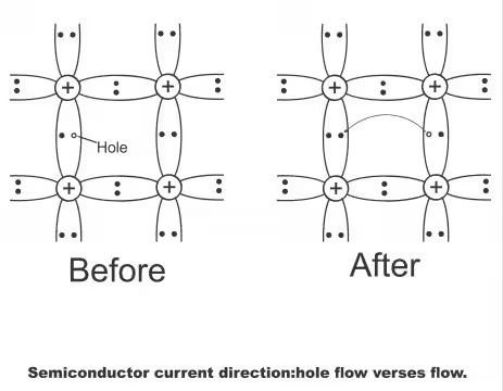
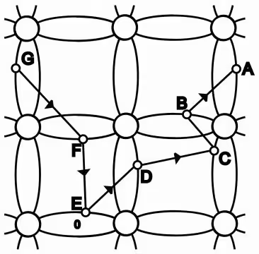
Suppose a hole is found in the rightmost side of figure 1.33 (b) (which results from movement of a valence electron into the conduction band through an increase in temperature from absolute zero. This hole attracts valence electrons present on hole “A”. Due to the influence of external source voltage, valence electron on “A” move towards hole and hole thus gets filled up due to the dropping of this valence electron. Thus, the original hole is filled, however a new hole generates on position A. This new hole on A attracts towards valence electron on position B, due to which electron present on B, moving towards the hole on A, fills it. Now a new hole come into effect at position B. When the valence electron moves from B towards A, the hole moves from A towards B (i.e. electrons and hole always move in opposite directions). Electrons keep on such a movement (Movement of valence electrons has been shown by arrow symbols in figure (b).Contrary to this, holes move in opposite directions i.e. from A to B and B to C. Thus, the process goes on and on(which can also be explained via figure 1.35).
Suppose, covalent bond breaks on point A. An electron from point A goes toconduction band via crystal and leaves behind a hole in the covalent bond. Electron on B jumps into the hole on A, after which electron of jumps into the hole on B, and this process moves on. Thus a hole develops on G due to the movement of electrons in turn, and a negative charged electron will move from G towards A. On the contrary, a positive hole will move from A towards G. The flow velocity of holes will be smaller than the flow velocity of electrons.
Energy Levels
Valence electrons proceed from valence band to conduction band due to the thermal energy ensuing from absolute zero temperature to a higher temperature. Thus, a free electron in conduction band and a hole in valence band is formed respectively (as shown in the diagram 1.33(c)) Conduction band free electrons move rightward due to a external voltage source, while hole in the valence band, moves leftwards. As several electron hole pairs develop due to thermal energy, we can thus, realize the concept of flow of free electrons from conduction band (rightward) and flow holes from valence band (leftward)
Holes Act Like Positive Charge
It may plainly be understood that a hole by itself is not a positive charge, as it is just a vacancy in the valance band, which is called hole. That’s it is a place, where a valence electron exists prior to proceeding to the conduction band. However, as a consequence of numerous experiments, it has been revealed that a hole moves and acts just like a positive charge. In order to understand, two methods of intrinsic conduction have been shown in figure 1.36. According to figure (a), free electrons and valence electrons both move towards right direction, while in the diagram (b), free electrons have been shown moving to right, while holes towards left.
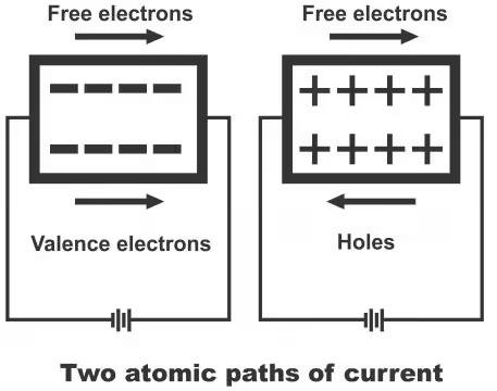
Free electron and valence electron move right
Free electrons move right and holes move left
Note; A semiconductor differs from a conductor because it is capable of the following two atomic paths.
- One is ordinary path, on which free electrons move found in the conduction band.
- An extraordinary path on which holes found in the balance band, move about. Due to the existence of such holes in semiconductor, manufacturers prepare diodes, transistors, ante grand circuits and all types of solid state (semiconductor) devices.
Extrinsic Types of Semiconductors
Intrinsic semiconductors which have some suitable variety of impurity or some quantity of doping agent (quantity is usually very small, i.e. approx. 8th part of108) is included, are called extrinsic or impure semiconductors. In other words, doped semiconductors are called extrinsic semiconductors. The doping agents, commonly are under:
- Pentavalent Atoms
Atom, which contains five valence electrons e.g. arsenic, antimony, phosphorus, bismuth. Such doping agents are also called pentavalent impurity.
- Trivalent Atoms
Atoms which contain three valence electrons, are called trivalent atoms, e.g. gallium, indium, aluminum and boron. Such doping agents are also known as trivalent impurity.
Pentavalent atom is also known as a donor atom, because it is donates an electron to a pure germanium conduction band. Contrarily, a trivalent atom is also known as an acceptor atom, because it accepts an electron from germanium atom.
Doping
- The operation of adding impurity to some pure semiconductor material, is called doping. Such a doped semiconductor is called impure or extrinsic semiconductor.
- The process by which impurity atoms are included intentionally or unintentionally, for changing or increasing the electrical conductivity of an intrinsic semiconductor is called doping.
- The process of changing the structure of pure semiconductor crystal through impurities, is called doping.
- The process of intentionally including impurity atoms in a pure semiconductor, so that its intrinsic characteristics could be changed, is called doping. The number of holes and electrons in a pure semiconductor is equal. There is an increase in electrons and holes, if impurity atoms are added to a pure semiconductor. Thus, its conductivity (ability to pass current) also increases. By doing so, important devices like transistors and diodes can be manufactured.
A vey small quantity of impurity atom is mingled with a pure semiconductor, normally between 106 to 1010. Only one atom of impurity is integrated in semiconductor (that’s the ratio of including impurity in a semiconductor is one atom per 10 6 to 10 10 atoms). The ratio of impurity in germanium is one to 10 8, while in silicon’s it is 10 12.
There are further two types of an extrinsic semiconductor on the basis of doping material applied in a pure semiconductor,
N-Type Extrinsic Semiconductor
P-Type Extrinsic Semiconductor
N-Types of Semiconductor
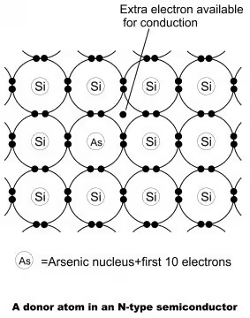
Amalgamation of some pentavalent material e.g. antimony or arsenic with a pure germanium or silicon crystal, results in N-Type Extrinsic semiconductor (as shown in figure 1.37). Every antimony atom, via coordination with 4 neighboring germanium atoms and 4 of its 5 electrons, build a covalent bond, while its 5th electron becomes superfluous and is slackly connected with antimony atom. Thus, via augmentation in thermal energy or setting up an electric field, this superfluous or extra electron can easily be excited to conductance band from valence band. Thus, every antimony electron in germanium atom or germanium lattice, practically presents a conduction electron or superfluous electron (without the creation of a positive hole). Antimony, is called donor impurity. Thus, through combining any pentavalent material (antimony, phosphorous, arsenic) with some pure germanium or silicon, extrinsic semiconductor gets developed (N means negative or minus). In the figure 1.38, arsenic has been shown to be combined with silicon crystal.

It should be kept into mind that donor atom, by means of sacrificing one of its valence electrons, becomes a positively charged ion, however it does not participate in conduction, because it is firmly fixed into the crystal structure.
Increasing the Free Electrons
We know that number of free electrons and holes all the time remain equal in some (pure) intrinsic semiconductor. When some pentavalent atom (e.g. antimony) is combined with a semiconductor (e.g. pure germanium or silicon), the number of conduction electrons in extrinsic semiconductor increase (resulting a reduction in holes). Similarly, when the concentration of electrons in conduction band increase (i.e. so many electrons collect in conduction band) and the concentration of holes in valence band increases (i.e. so many holes get collected in valence band), Fermi level gets nearer to conduction band via raising a little. In case of intrinsic semiconductor, Fermi level is located right in the middle of valence band and conduction band. (Fermi level reflects the energy level between conduction band and valence band,via which weighted center of gravity between conduction electrons and holes builds upon the basis of their energies), as number of charge carriers in conduction band exceeds those on hand in the valence band(displayed via figure 1.39)

From the energy level perspective, energy level of the 5th antimony electron (also called donor energy level) is located right below the conduction band. Normally, donor level’s value beneath the conduction band, for germanium is 0.01eV, while for silicon; its value uses to be 0.054eV.
It is obvious from the above description that electrons in N-Types of semiconductors are majority carriers while holes are minority carriers. I.e. free electrons are known as majority carriers whereas holes as minority carriers. It has also to be bear in mind that despite being in majority, electrons in semiconductors are neutral (impartial with regard to electricity). It is due to the fact that the number of electrons available for conduction purposes as a result of combining impurity, is greater than intrinsically available holes. However, the cumulative charge of semiconductors does not change, because the negative charge which donor impurity produces, brings about an equal charge (through electrons by the way of electrons present in its nucleus)
P-Types of Semiconductors
When a trivalent impurity (e.g. boron) is integrated into some pure germanium (or silicon), we get P-Type semiconductors.
In such a case, 3 valence electrons of boron atom by combining with of 4 germanium atoms found close by, produce 3 covalent bonds, while one bond remains incomplete. (displayed in diagram 1.41 “a”)
Thus, a number of positive holes develop by means of combining boron(also called as an acceptor impurity) with germanium crystal. Thus, for the acquisition of P-Type extrinsic semiconductor (P means positive), trivalent impurity (e.g. boron, aluminum or indium) is combined to some unadulterated germanium or silicon crystal.

The conduction operation in such semiconductors occurs via holes in the valence bands (flow of holes current in N-Type semiconductors is slower compared to the electron current). Therefore, holes act as majority carriers while electrons as minority carriersin a P-type semiconductor. As the number of holes in valence bands exceeds the number of electrons in the conduction band, therefore, fermi level shifts closer to the valence band (shown in figure 1.41 “b”). Acceptor level immediately move above the fermi level. Due to the movement of conduction holes on valence bands, the process of conduction occurs and acceptor level immediately accepts electrons from the valence band.
The number of holes in P-type semiconductor is huge for the purpose of conduction, despite this it is precisely electrically neutral like an N-type semiconductor (already explained in N-type semiconductors’ section)
Majority and Minority Carriers
No free charge carriers are found on a piece of uncontaminated germanium or silicon at 0⁰K, however, as its temperature is increased (up to room temperature), some of its covalent bonds break up due to heat energy, due to which electron hole pairs are generated. These are called thermally generated charge carriers or also called intrinsically accessible charge carriers. Normally, their number is very small. Intrinsic of a pure germanium can be converted to a P-type semiconductor by means of including an acceptor or trivalent impurity, due to which a large number of holes are produced within it. Thus, a P-type material contains the following charge carriers.
(a). A large number of positive holes -majority of which generate via combining some kind of impurity, whereas number of holes, generated through the thermal heat, is small.
(b). A very small number of thermally generated electrons – Normally, number of holes (generated both through adding impurity and via heat) in a P-type material exceeds the number of electrons. Thus, in such type of material, holes are called majority carriers whereas electrons are minority carriers. (figure 1.43 “a”)
Similarly, number of electrons (generated both through an addition of some kind of impurity and thermal heat) exceeds the number of thermally generated holes in a N-type material. Thus, in such type of material, electrons are called majority carriers, whereas holes are called minority carriers.

For electronics and programming related projects visit my YouTube channel.
Previous article: Semi-Conductors and Next article: PN Junction
Discover more from Electronic Clinic
Subscribe to get the latest posts sent to your email.
