Biasing of JFET: Gate Bias, Self Bias, Voltage Divider Bias, Source Bias, Current Source Bias
Last Updated on September 6, 2022 by Engr. Shahzada Fahad
Table of Contents
Biasing of JFET:
We know that the input resistance of a JFET is quite high compared to a bipolar transistor. Therefore, it should inculcate in mind that at the time of JFET biasing, its input resistance should in no way get lower. Therefore, for the achievement of this objective, the gate-source diode of a JFET is always revere-biased. Thus, negative Vgs is required for biasing an N channel JFET, whereas positive Vgs is needed for biasing P channel JFT. Contrarily, if the gate-source of JFET is forward biased instead of reverse bias, its high input resistance will drop suddenly. Thus, this device will lose its advantage due to which it has a preference over a BJT.
A JFET can be biased in the ohmic or active regions. When it is biased in the ohmic region, it is equal to the resistance. However, when it is biased in an active region, it becomes equivalent to a current source.
The methods commonly used for JFET biasing are as follows:
1). Gate Bias
2). Self-Bias
3). Voltage Divider Bias
4). Source Bias
5). Current Source Bias
Gate Bias
In this method of biasing, the negative gate voltage (-Vgg) is provided to the gate through biasing resistor (Rg), while the source of JFET is earth (figure 5.18 a). In this method, as the bias voltage is supplied on the JFET gate, therefore, this method of biasing is called gate biasing. Drain current sets up due to providing a negative bias voltage to the gate, the value of which is lower than Idss. When this drain current passes from Rd, drain voltages are generated parallel to it, values of which are as below.
Vd= V dd– I d R d
This method of JFET biasing in an active region is quite unpopular because point Q becomes highly vulnerable/unstable due to gate biasing. However, the method is preferred for biasing in the ohmic region instead of the active region, because, the issue of stability of the Q point does not arise in the ohmic region.
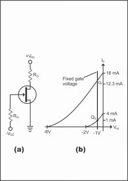
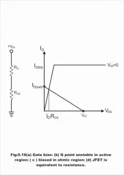
Figure 5.18 (a). Gate bias (b). Q point unstable inactive region (c). biased in the ohmic region (d). JFET is equivalent to resistance
In figure (b) minimum and maximum trans-semiconductor curves of a JFET 2N5459 have been shown while operating its inactive region. In such a situation, Idss value varies between 4-16 mA, and Vgs (off0 value varies between-2 to -8. If the gate bias value of this JFET becomes -1V, we get minimum and maximum Q points as has been illustrated in the figure. Thus, under such a situation, the drain current of Q1 is 12.3mA and the value of Q2 drain current is just 1mA. In figure (c) a JFET has been shown to be biased in the ohmic region. The upper end of the DC load line is capable of drain saturation, the value of which is as below:
ID (sat)=VDD/RD
Remember, when a JFET is biased in the ohmic region, the value of Vgs is retained at zero (i.e. Vgs=0) and ID (sat) value is far lower compared to IDSS i.e.
ID (sat)<< IDSS
The equation reflects that the value of drain saturation current has to be significantly lower compared to maximum drain currents’ value i.e. if a JFET’s IDSS value is 10mA, hard saturation results in case Vgs value is considered as zero and ID (SAT) value 1mA.
When a JFET is biased in the ohmic region, t is reflected vide a resistance RDS (i.e. JFET is converted to RDS) as shown in figure (d). According to the figure, JFET is fixed in RD series treating JFET equivalent to RDS resistance. Through such equivalent circuits, drain voltages can be calculated. When RDS value is lowest compared to RD, the value of drain voltages approximates zero.
From the above discussion, it has been proved that such type of bias is considered extremely unstable. Its other major defect is that if the biasing value of VGS is other than zero, another or one more power supply will become imminent under the situation. Thus, the application of this biasing method equals almost nothing.
Self-Bias
In this biasing method, a power supply is just provided on the drain, where no power supply exists on JFET’s gate (figure 5.19). Gate resistor RG does not affect bias at all, because no voltage drop occurs parallel to it. As the gate has been grounded through resistance RG, therefore, the gate remains on zero voltage. The application of RGS for isolating AC signals from the ground is essential while using JFET as an amplifier (Read details in the coming pages). Current source resistance passes through Rs due to which voltage drop takes place parallel to Rs. Therefore, the voltage drops which occur parallel to Rs in this biasing method, perform the function of gate-source voltage.
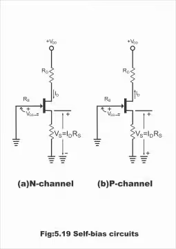
When source current Is passes through N channel JFET’s source resistance as shown in figure (a), voltage drops form parallel to Rs, which makes the source positive with respect to ground. As drain current pass through source resistor Rs, and values of source current and drain current are equal (i.e. IS=ID), further as the value of gate voltage (Vg) is zero, thus, in this case, source voltage VS equals the product of drain current and source resistance (RS)i.e. VS=ID RS. However, the value of gate to source voltage is as under:
VGS =VG -VS=0 – IDRS
VGS = -ID RS …… (N-Channel)
According to the equation, it is evident that gate-source voltage equals the negative voltage found parallel source resistor. Basically, this circuit generates bias for itself via providing reverse bias to the gate as a result of negative voltages produced parallel to RS. In the case of P-channel JFET, the current passing through RS, causes a negative voltage on the source (as shown in figure b). Thus, the value of VGS is as follows.
VGS = +ID RS ……. (P-Channel)
Drain voltage value with respect to ground is as under
VD = VDD-ID RD
As, VS = ID RS, thus, drain to source voltage equals the following
VDS = VD – VS
Entering the values of VD and VS in the above equation
VDS= VDD-ID RD-IDRS
VDS= VDD-ID (RD+RS) …(N-Channel)
VDS= -VDD+ID (RD+RS) …(P-Channel)
Remember, self-biasing also works as feedback. When draining current increases, source current also increases (as IS = ID), due to which drop in RS also increases. As this bias provides reverse bias voltage to gate-source diode, therefore, reverse bias on gate-source diode also increases with an increase in drop parallel to RS. which results in lowering drain current. As the Q point in self-biasing is not so stable compared to other biasing methods, therefore, only small-signal amplifiers are self-biased, whereas, for high signals, other types are used for biasing a JFET. Self-bias JFET circuit is mostly used on the front part of communication receivers (where a small signal exists)
Voltage Divider Bias
In this biasing method, Thevenin voltages are supplied to the gate by fixing two resistors on the gate. In diagram 5.20, a voltage divider bias circuit has been shown. As its name suggests, the value of bias voltage or gate voltage is reduced to such an extent by dividing it into two parts with the help of two resistors, that their value remains a fraction compared to supply voltage (i.e. gate voltage is equalized just to a fraction of supply voltage)

According to the diagram, gate voltage (VG) is set through R1 and R2, values of which according to the voltage divider formula is as follows:
VG = V1h [R2/R1+R2] VDD
Thus, we get the following voltage parallel to the source resistor or between ground and source.
VS= VG – VGS
As VGS is negative, therefore, source voltages are relatively higher as compared to the gate voltage. When source voltages are divided by source resistance, we get drain current (which is equal to source current) i.e.
ID = VG -VGS /RS = V1h -VGS/RS
If the value of VGS is higher significantly relative to VG or Vih, the drain current of nearly every JFET normalizes as shown in diagram 5.20 b). However, as VG varies extensively from transistor to transistor, therefore, ID might have various possible values. Remember that voltage divider bias can establish a strong Q point due to the presence of large gate voltage compared to VGS(the middle point of intersection between a straight line and trans-conductance curve, is called the Q point). Although voltage divider bias is more stable as compared to self-bias, nonetheless, this method of biasing is not so balanced as compared the bipolar transistor.
For clarification, separate voltage divider bias circuits of N-channel and P-channel JFET have been shown in diagram 5.21.

Source Bias
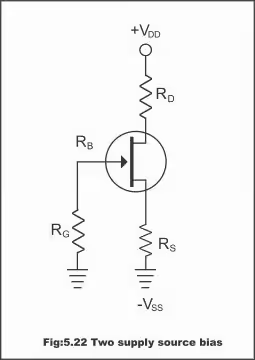
The source bias method is applied for eliminating variations in VGS as far as possible (this biasing method is also called two supply source bias). In this method, VSS value is increased excessively as compared to VGS. In figure 5.22, a source bias circuit has been illustrated. Practically, the value of drain current will be as follows
ID = VSS – VGS/ RS
In a typical situation, drain current is achieved by dividing supply voltage (VSS) by source resistance (RS). i.e.
ID= VSS/ RS
Under such a situation, the value of drain current remains almost constant despite changing JFET and temperature. As VSS value is much higher relative to VGS (which normally remains between -1V to -5V), therefore, comparatively better results can be achieved through source bias.
Current Source Bias
In current source bias, a bipolar transistor functions as a constant current source for generating a fixed value of drain current. When the drain supply voltage is not too large, a suitable gate voltage value also does not exist for avoiding variations in VGS. In such a situation, the designer prefers the application of current source bias 9its circuit displayed via diagram 5.23 a)

A bipolar transistor has been used in the circuit, on the emitter of which, bias is supplied. Thus, a fixed current pass through JFET. Therefore, the value of drain current in such a situation will be as under.
ID = VEE-VBE/ RE
As junction transistor works in the capacity of the current source, therefore, it strives to equalize JFET drain current to its collector current (i.e. ID = IC). In the case of a constant IC value, the drain current value also remains constant. Thus, the impact of variations on VGS due to current source bias becomes ineffective and consequently, JFET operates in a balanced manner.
In figure (b) it has been shown how effective current source bias is. According to the diagram, despite different VGS values for each Q point, both Q points have the same current capacity. It implies that there is no worthwhile impact of VGS on the value of drain current. Thus, compared to other biasing methods, current source biasing forms the most stable Q points because drain currents’ value stays uniform in spite of variations in JFET characteristics.
Uses of JFET
Junction Field Effect Transistor is mostly applied as amplifiers and analog switches. Therefore, these are commonly used in multiplexors, chopper amplifiers, buffer amplifiers, voltage controller resistors, automatic gain control (AGC) circuits, cascade amplifiers current sources, and current limiters.
Previous Topic: JFET: Junction Field Effect Transistor
Next Topic: FET as a Voltage Amplifier
For electronics and programming-related projects visit my YouTube channel.
Discover more from Electronic Clinic
Subscribe to get the latest posts sent to your email.
