JK Flip-flop: Positive Edge Triggered and Negative Edge-Triggered Flip-Flop
Last Updated on November 21, 2022 by Engr. Shahzada Fahad
Table of Contents
JK Flip-flop
A type of flip-flop that can operate in set, reset, no change and toggle modes by means of having characteristics or attributes of all other types of flip-flops, is called a JK flip-flop. JK flip-flop is an amended form of RS flip-flop and it is also free from the defect of race condition (both outputs becoming high at a time is called race condition). However, a difference still exists between a JK flip-flop and an RS flip-flop. JK flip-flop consists of three whereas RS flip-flop 2 inputs. Besides, another basic difference between the two is that RS flip-flop consists of a single feedback circuit whereas JK flip-flop consists of a double feedback circuit. JK flip-flop is a versatile and probably most widely used flip-flop. In a JK flip-flop, J & K refer to two inputs, similar to R and S are two inputs in an RS flip-flop. The operational mechanism of a JK flip-flop is also similar to that of an RS flip-flop, the only difference being that contrary to an RS flip-flop, no invalid state exists in a JK flip-flop. If both inputs of a JK flip-flop are presumed to be set or reset similar to an RS flip-flop, its operation can be understood quite easily (i.e. K = R = Reset = and J = S = Set). A JK flip-flop is an ideal memory element which can be used for counting purposes. It has vastly been used for manufacture of counters. As this flip-flop possess features of flip-flops of all other types, that is why it is generally known as a universal flip-flop. These flip-flops are both positive edge-triggered as well as negative edge-triggered.
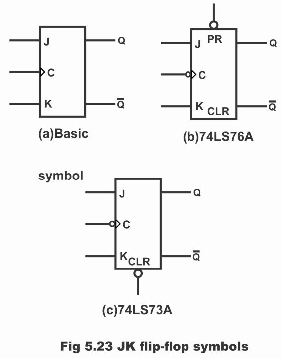
In figure 5.23, various symbols of a JK flip-flop have been depicted. The symbol shown in figure (a), represents a symbol for any type of flip-flop. Whenever somebody happens to see such a symbol on any circuit diagram, following points will certainly come into mind.;
(1). When both J and K inputs are low, no change occurs in Q
(2). When J is low and K is high, output Q tends to reset or turn low
(3). When J is high and K is low, Q gets set or becomes high
(4). When both J and K are high, Q toggle on inverted states
The symbol shown in figure (b), represents a JK flip-flop which contains two additional characteristics of preset and clear. Remember that it is a negative edge-triggered flip-flop which requires low PR for being set or low CLR for being reset. Output Q shows an immediate reaction on PR and CLR signals.
In figure ©, another commercially available JK flip-flop has been demonstrated. This is a negative edge-triggered flip-flop, for which CLR has to be brought low in order to reset it. It should be kept into mind that both PR and CLR are asynchronous and they invalidate or reject all other operational input signals.
Figure 5.23-JK flip-flop symbols
Positive Edge Triggered Flip-flop
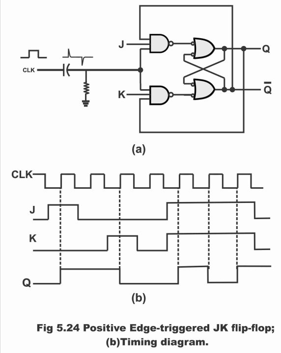
In figure 5.24, logic diagram of a positive edge triggered JK flip-flop along with its timing diagram has been denoted, wherein two data inputs J and K are also visible besides clock input. Here, a short time constant circuit along CLK input has been demonstrated, which converts quadrate-type clock pulse into narrow spikes, as has been depicted in the diagram. It is obvious from the logic diagram that Q output has been connected or feedback with bottom NAND gate whereas Q output connected with top NAND gate (that’s JK flip-flop is a double feedback circuit). This circuit is a positive edged-triggered circuit owing to a double inversion via NAND gates. In other words, inputs are enabled (or operate) only on the rising edge of the clock.
Figure 5.24-positive edge-triggered JK flip-flop (b). timing diagram
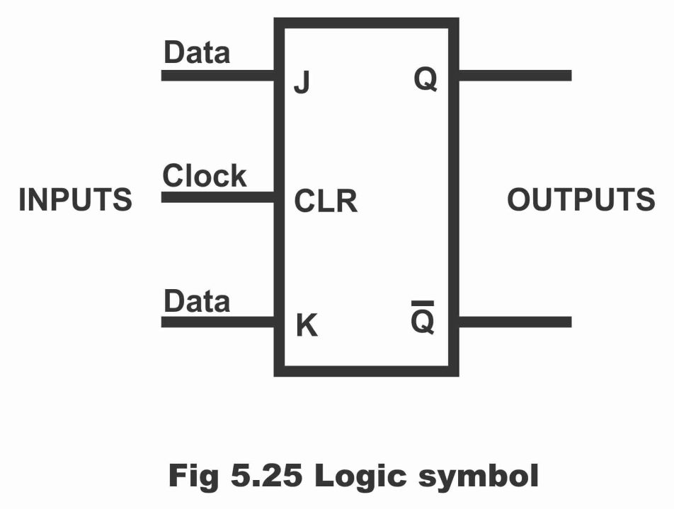
In figure 5.25, logic symbol and truth table for a JK flip-flop have been illustrated. In the logic symbol, J and K implies data inputs and CLK input means clock input. Whereas as usual, Q and Q are normal and complementary outputs respectively.
Figure 5.25-JK flip-flop (a). logic symbol (b). truth table
According to truth table shown in figure (b) complete operation of a JK flip-flop can easily be comprehended by means of dividing it into the following parts.
(1). When J and K both inputs are low or 0, both input gates turn out to be disabled (i.e. do not operate). Under such a situation, flip-circuit remains inactive or in hold mode in spite of being on the rising edge of the clock. As such data inputs (J & K) have no impact whatsoever on outputs (Q & Q). Thus, no change occurs in output (i.e. previous or last data survives on outputs in situation of a hold state). This can be seen via first line of the truth table.
(2). When value of J is 0 and K’s value is 1 or when J input is low and K input is high, top gate turns out to be disabled (i.e. does not operate) and bottom gate turns enabled (i.e. start to operate). Therefore, it is possible just to reset a flip-flop instead of having it set. When Q output is high, as soon as the positive clock edge arrives, bottom gate passes a reset trigger, resultantly Q output turns low and a rising clock edge resets flip-flop (i.e. a reset state develops on flip-flop) as can be seen via line number 2 of the truth table.
(3). When J input is high and K input is low (i.e. J = 1, K = 0), the bottom gate turns disabled and top gate becomes enabled. Thus, it is possible just to set a flip-flop instead to reset it. When Q output is low and Q output is high (previous flip-flop state or reset state), then in such a situation top gate passes a set trigger upon arrival of a positive clock edge, due to which output Q turns into high (i.e. next positive clock edge, sets flip-flop) as has been demonstrated vide line 3 of the truth table.
(4). When both J and K inputs are high (remember that in case of RS, it is reflecting a prohibited state) output tends to turn on or off continuously as a result of advent of clock pulses so repetitively. As this on-off action is similar to a toggle switch, therefore this operation is called toggle. Thus, in such a situation flip-flop remains in its toggle mode. In other words, when both inputs are high, if value of Q is 0, then bottom gate becomes disabled, however top gate turns out to be enabled. As a consequence, flip-flop sets. On the contrary if Q value become 1 when both inputs turns high, then bottom gate enables and top gate becomes disabled (absolutely converse to the above-mentioned state). As a consequence, flip-flop resets. It means that flip-flop toggles by means of clock pulses when both inputs are high (i.e. sometimes its output is high, sometimes it is low or it turns on-off repeatedly). As such it is possible to set or reset a flip-flop in the event both inputs J and K are high. However, set or reset depends on present state of output. if Q is high, then bottom gate passes a reset trigger or pulse upon arrival of the next positive clock edge. Inversely, when Q output is low, top gate passes a set trigger upon arrival of the next positive clock edge. As such, in both situations, flip-flop output Q changes according to complement of its previous or last state. That’s to say if Q value is 1, it becomes 0 and if Q value is 0, it turns out to be 1. Thus, J = 1 and K = 1, means that flip-flop will toggle upon arrival of next positive clock edge (toggle means adoption of an inverted state)
In figure 5.24 (b), timing diagram represents summary of a JK flip-flop’s entire operation. it is evident from this diagram that when J input is high, and K input is low, then rising clock edge sets Q on high. Conversely, when J input is low and K input is high, then rising clock edge resets Q on low. However, when both J and K inputs are high at a time, output toggles on every rising clock edge. This has been shown vide the last three vertical dotted lines of the timing diagram. Thus, as a result of timing feature of a JK flip-flop, race condition drawback or defect eliminates completely. In other words, this kind of defect is not found in this flip-flop (toggle occurrence more than once during a clock cycle is called racing)
Negative Edge-Triggered JK Flip-flop
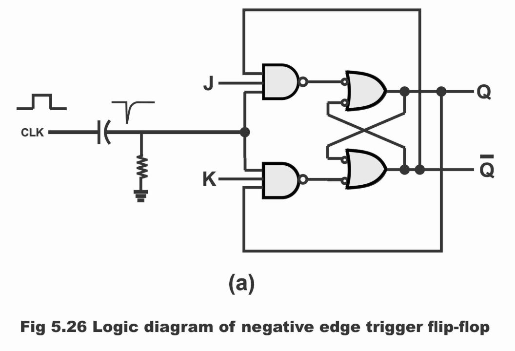
In figure 5.26 (a), logic diagram of a negative edge-triggered JK flip-flop and in figure 5.26 (b) its truth table has been shown. As this flip-flop operates only on a negative- going clock pulse (i.e. changes its output state), therefore it is called negative-edged-triggered flip-flop. It ought to be remembered that output of this type of flip-flop changes only on a falling edge or negative edge of the clock.
Figure 5.26 (a) logic diagram of a negative edge trigger flip-flop (b). truth table
Operation
According to truth table shown in figure (b), this type of flip-flop operates in following manner;
(1). When clock is low or high or on its positive going edge, in such a condition flip-flop does not operate (i.e. it remains inactive). This has been displayed through first three lines of the truth table. As a consequence, no change take place in Q output.
(2). When both control inputs J and K are low, even then circuit does not activate, thus output also does not change. This has been illustrated via line 4 of the truth table.
(3). When J input is 0 while K input is 1 (i.e. J = 0 and K = 1), then value of normal output Q becomes 0 value of complement output Q turn out to be 1 on the arrival of clock pulse ‘negative going edge. Hence, flip-flop resets, as has been shown via line number 5 of the truth table.
(4). When input J and input K both are 0 (i.e. J = 0 and K = 0) then clock pulse ‘negative going edge sets flip-flop. As a result, Q output becomes 1 and Q output turns out 0, as has been displayed in line number 6 of the truth table.
(5). In case both inputs are 1, (i.e. J = 1, K = 1) then both outputs Q and Q toggle with each passing negative-going clock edge. This operation of flip-flop has been depicted via last line of the table.
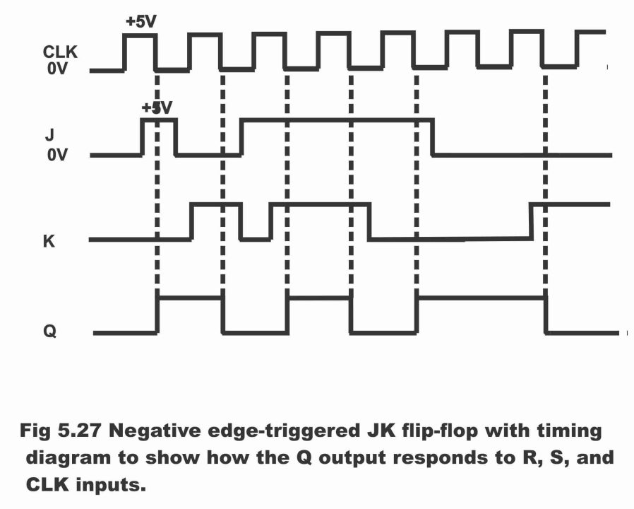
For further clarification, it has been elaborated via the timing table shown in figure 5.27, that how output Q changes as a consequence of interaction between JK and CLK inputs.
Figure 5.27-negative edge -0 triggered JK flip-flop with timing diagram to show how the Q output responds to R, S and CLK inputs.
Preset and Clear Facility in JK Flip-flop
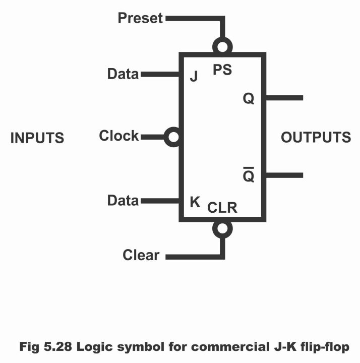
Commercially available JK flip-flops (which are available in ICs form) contain two additional inputs i.e. preset (PS) and clear (CLR), which are known as asynchronous inputs. These asynchronous inputs relinquish or reject synchronous inputs (J & K) as and when required. Normally, PS and CLR are capable of active low status. It means that they are normally high however, whenever the circuit is desired to be preset or cleared, they are momentarily turned low. By means of pressing low preset push button, Q value becomes 1 and pressing low clear button, Q value turns out 0. It has to be remembered that whenever a computer is logged on, operator press a master reset button, which transmits a clear (reset) signal on all flip-flops. Further, it is essential in some computers that certain definite flip-flops be pre-set prior to operation of the computer.
In figure 5.28 (a), logic symbol of a commercial TTL 7476 JK flip-flop has been illustrated, wherein two asynchronous inputs (Clear and Preset) are also present besides synchronous inputs (J and K). In this symbol, normal output Q and complementary output Q can also be seen. In figure (b) truth table of this flip-flop has been depicted, which reflects that these synchronous inputs (CLR and PS) invalidate synchronous inputs (CLR and PS) as can be observed through first three lines of the truth table. Because according to these three lines, asynchronous inputs are activated. That’s the reason synchronous inputs (CLK, K and J) within the first three lines have been represented by X sign by declaring them irrelevant. When both asynchronous inputs are activated simultaneously, prohibited state builds up. Remember that this state is not at all conducive, therefore such a state must always be refrained (i.e. flip-flop should never be operated in this type of state)
Figure 5.28-(a). logic symbol for commercial J-K flip-flop (b). truth table for 7476 J-K flip-flop.
When both asynchronous inputs do not operate, they are in its normal condition at that time (i.e. high or 1), then in such a situation synchronous inputs can be activated. The bottom four lines of the truth table have been elucidating hold, reset, set and toggle mode of operation of a JK 7476 flip-flop. JK flip-flops are used in a number of digital circuits. these are particularly used in counters, whereas counters are found nearly in all digital systems. JK flip-flops are available both in TTL- IC and CMOS – IC form. 74HC76, 74AC109 and 40271C are specific JK CMOS flip-flops.
Previous Topic: D Flip-Flop and Edge-Triggered D Flip-Flop With Circuit Diagram
Next Topic: Trigger in Flip-Flop with Circuit Diagram in Digital Electronics
For electronics and programming-related projects visit my YouTube channel.
Discover more from Electronic Clinic
Subscribe to get the latest posts sent to your email.

