D Flip-Flop and Edge-Triggered D Flip-Flop With Circuit Diagram And Truth Table
Last Updated on November 21, 2022 by Engr. Shahzada Fahad
Table of Contents
D Flip-flop
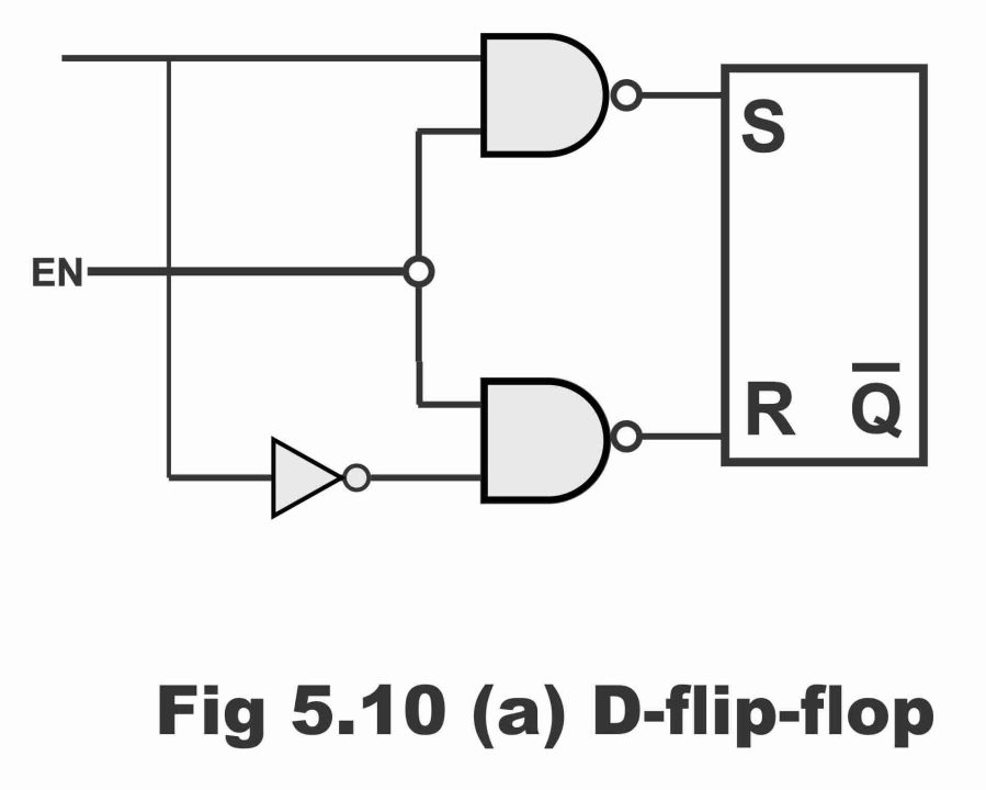
A flip-flop circuit, which need just a single data input, is known as a D flip-flop. In other words, a D flip-flop (also known as data flip-flop or gated D latch or D type latch) consists of a single data input, apart from a clock input. When an inverter is fixed alongside an RS flip-flop, an elementary D flip-flop come into existence, as has been revealed via figure 5.10. When a single data bit (0 or 1) is desired to be stored, D flip-flop proves very useful for this purpose.
Fundamentally, D flip-flop is a modified form of an RS clocked flip-flop as can be observed via figure 5.11. It is quite obvious from the figure that this flip-flop consists of input D (which is called data input) apart from clocked or enabled input. This D input converges straight on to S input and a complement of D input is received on R input via a NOT gate or inverter. D flip-flop is also known as a delay flip-flop, because its input data (0 or 1) transmits on output after some delay equivalent to an interval of a clock pulse.
Figure 5.11 – A D flip-flop
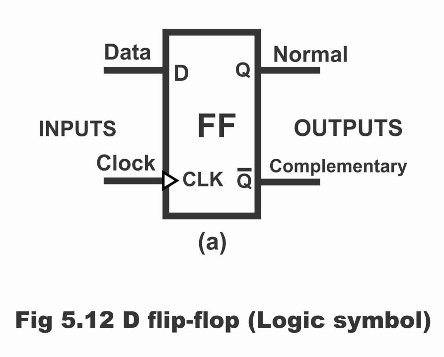
We know that RS flip-flop comprises two data inputs i.e. R and S. In order to store a high bit on to it, application of a high S and to store a low bit, a high R is imminent. Thus, two signals S and R are required in order to operate a flip-flop. The creation of two signals in order to drive a flip-flop, is quite damaging in several of the applications (here just keep in mind Q output and forget about Q output for the time being). Another disadvantage of an RS flip-flop is that a prohibited or forbidden state builds up on it when both of its inputs R and S are inadvertently turn out high (it is also known as race conduction). Owing to these two significant drawbacks, an RS flip-flop fails to cast a positive impact on several of the applications. A D flip-flop has been designed in such a way that it requires just one single data input. Therefore, a D type flip-flop is completely absolved of both these types of faults, because an inverter guarantees that S and R will always be in a converse state, therefore formation of a race conduction in D flip-flop is virtually impossible. Thus, a D flip-flop is a kind of bistable circuit, the input data of which just transfers on output when EN or CLK inputs is high. In figure 5.12, logic symbol and its corresponding truth table has been displayed. Figure (a) just comprises a data input D and clock input CLK, whereas outputs are Q and Q. As data (0 or 1) provided on input D is received on output Q after a delay equivalent to a clock pulse, therefore output Q shown through the truth table in figure (b) has been represented by Qn+1. Hence, this type of flip-flop is also generally known as a delay flip-flop. It is clear from the truth table that input data (0 or 1) transmits on output in case of a high CLK input (i.e. when CLK input is high or enabled, binary information existing on data input of D flip-flop, transfer on output Q). However, it is to be reminded here that input data is received on output as long as clock pulse remains high or 1. When clock pulse turns out to be zero or low, at that time when pulse continues changing from high to low, information on data input is unceasingly being received on output Q, until clock pulse enables once again.
Figure 5.12 – D flip-flop (a). logic symbol (b) simplified truth table
The operational process of D flip-flop shown in the figure 5.11 is as follows:
When value of EN is low, both AND gates are disabled (i.e. they stop operating). Therefore, value of data input D has no impact on output Q whatsoever (i.e. whatever the value of D, this value is not at all received on output). on the contrary, when EN is high, both AND gates are enabled (i.e. they start to operate). In such a situation, output Q value becomes equal to the value of input data D (i.e. Q = D) which means that data present on input, transfers to output. However, when EN value lowers once again, then last D value transmits on Q. In other words, data bit changes at a time when EN is high, then prior to EN gets low once again, the last D value is considered as stored value of D.
In figure 5.13, truth table of this D type flip-flop or D latch has been demonstrated, which has been offering an all-inclusive explanation of the aforementioned process. It is evident from the first line of the table that when EN value is low, D flip-flop remains in an inactive state (i.e. it does not operate). This state has been mentioned in the table by “X” or “do not care”. In such a situation, Q retains its last state or it latches on its last state. However, when EN is high, then last value of D appears on Q. At a time when the value of D has been changing, and during the meantime EN gets high, then only last value of D is being treated as a stored value.
Figure 5.13 – truth table for D type flip-flop
Remember that when clock is low, then circuit gets latched and hence Q output does not change. However, when clock is high, Q value becomes equivalent to D. and when D is high, Q also turns high, however D gets low, Q also becomes low. As such D flip-flop or D latch is a transparent latch, which means that during high clock, output of this latch is according to or equal to the value of D. Thus, D flip-flop is a form of a bistable multi – vibrator, wherein output follows input D state (0 or 1) or values of output and input “D” are same or jointly equal.
Level Triggering & Edge Triggering
D flip -flop which has effusively been described above, is a level clocked device (i.e. output of this device changes only when clock is high or low). As a number of issues and defects have been witnessed as a result of application of level clocking, therefore edge triggering mechanism has generally been preferred over level clocking. According to which, output condition of a flip-flop changes only when clock pulse is on its rising or falling edge. In other words, when a circuit is edge-triggered, its output changes only on rising or falling edge. It further means that when square shaped clock pulse is on positive going edge (i.e. in descending form) output changes. A D-type flip-flop which changes its output on positive going edge, is called positive edge-triggered flip-flop. And a D type of flip-flop, which changes its output on negative going edge, is called negative edge-triggered D flip-flop.
In short, when circuit is activated through transition portion of a clock, it is called edge-triggering. However, when the circuit is activated via voltage level, it is known as level triggering. In order to fully comprehend edge-triggering, a square wave has been illustrated in figure 5.14 (a), which represents a full cycle of clock pulse. This whole cycle can be divided into following different portions.
Figure 5.14

a → b = +Ve edge or rising edge or positive transition
b → c = high level
c → d = -Ve edge or falling edge or negative transition
d → e = low level
According to this figure, a to b and c to d portions are transition portions of this clock pulse, or in other words clock changes positions within these portions or clock continues to remain on its changing status. Low to high transition is frequently considered as a positive transition (PT) and high to low transition is called negative transition. This has been illustrated in figure (b). A circuit which changes its state on PT, is called positive edge triggered and a circuit, which changes its state on NT, is called negative edge triggered.
Remember that capacitive coupling is being resorted to in order to enable a flip-flop to act on plus transition. Capacitive coupling consists on a RC (resistor-capacitor) circuit. This RC circuit is being combined with the flip-flop’s clock input. According to the working mechanism of an RC circuit, capacitor fitted inside the circuit allows AC to pass through it, whereas it blocks DC.
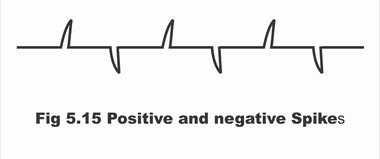
For example, as “ab” portion of clock pulse shown in figure (a) is AC, therefore when this portion passes through the capacitor, it charges the capacitor. As a result, a narrow thin positive spike is produced parallel to the resistor. When “bc” portion of the clock pulse strikes, capacitor blocks it, because it is “dc” portion. When “cd” portion comes, it also goes through capacitor as a result of being AC, thus a thin negative spike is produced. In figure 5.15, these positive as well as negative spikes have been illustrated. Both these positive as well as negative spike are used in order to enable gates on a flip-flop circuit. As flip-flop operates when clock is in its changing status, therefore this kind of operation is called edge triggering. It must also be kept in mind that a flip-flop circuit is being designed in such a fashion that it can accept just one spike (either positive or negative) at a time, while it repudiates other spike. A flip-flop which accepts a positive spike is called positive edge-triggered flip-flop. And flip flop, which accepts negative spike, is called negative edge-triggered flip-flop.
Figure 5.15 – positive and negative spikes
Edge-Triggered D Flip-flop
A D type flip-flop, wherein data penetrates via rising or falling clock pulses and which is received on output, is called edge-triggered D flip-flop. In other words, edge-triggered D flip-flop is a kind of flip-flop, wherein data (D) is triggered on a positive edge (or negative edge) of clock pulse or on to the transition portion of the clock pulse (remember that providing of clock pulse on a circuit is called triggering).
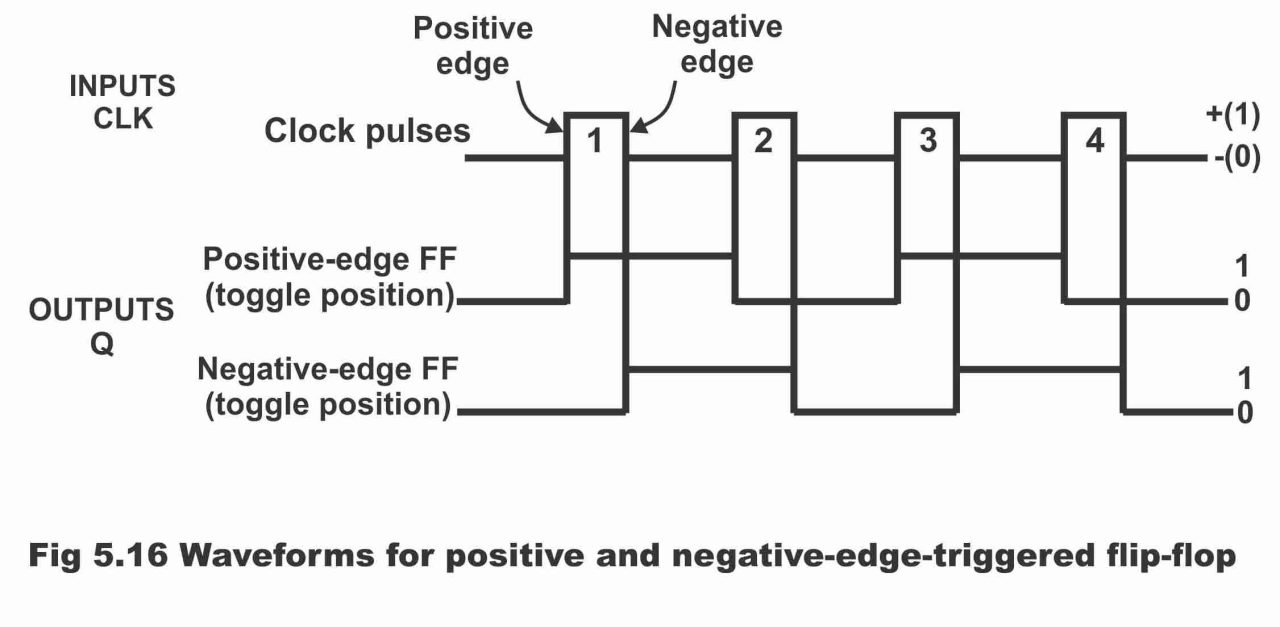
In figure 5.16, two edge-triggered D flip-flops have been demonstrated in a toggled position. The identification of positive edge or positive going edge and negative edge or negative going edge has been shown on clock pulse 1. Other wave form of this figure indicates that as to how a positive edge flip-flop always toggle upon striking of a positive going pulse (pulses from 1 – 4 in the figure). In this figure, role of a negative edged or a negative going edge has also been demonstrated, which can be seen via the bottom most wave form. The bottom most wave form indicates that how a negative edged flip-flop toggles upon advent of a negative clock pulse (i.e. how does a negative edge flip-flop trigger as a result of receiving a negative pulse). In the figure, this state shifting process or toggle as a result of receiving a negative going pulse every time, has been represented by pulse 1 – 9. Here, an important thing which needs to be reminded is the timing difference between positive and negative edged-triggered D flip-flop, because this triggering time difference has substantial implications on some of the applications. However, it has also got to be remembered that positive edged-triggering D flip-flops are mostly being used these days in spite of numerous flaws.
Figure 5.16 – waveforms for a positive and negative edge-triggered flip-flop
Positive and negative triggering is normally being explicated above a flip-flop. In figure 5.17, logic symbol of a positive edge triggered D flip-flop has been illustrated, in which a triangular sign has been displayed near the clock input inside the flip-flop. This sign reveals that data has been transferred on to output via a pulse edge. In other words, presence of a tiny triangle on clock input indicates that flip-flop edge has actually been triggered. In figure (b), logic symbol of a negative edge D flip-flop has been illustrated. In this figure, a small circle or bubble has been drawn above the clock input, which signifies triggering having been occurred on negative going edge of the clock pulse.
Figure 5.17 – (a). logic symbol for a positive edge-triggered D flip-flop (b). logic symbol for a negative edge-triggered D flip-flop

For further clarification, a RC circuit has been shown being mounted along the D flip-flop input. In this design, RC timing constant has intentionally been kept very low as compared to clock pulse width, so that when clock is high, capacitor could be fully charged during the period. As a result of this charging process, a narrow thin positive voltage spike is generated parallel to the resistor. After this, a thin narrow negative spike is also produced as a result of negative edge or trailing edge of the clock pulse.
Figure 5.18

Narrow positive spikes happen to enable input gates momentarily, however narrow negative spike has no viable function to perform. As such, input gates activate during a positive spike (i.e. they start functioning) and during that time, input data D and its complement, either set or reset output Q by means of striking the flip-flop inputs. This type of operation is called edge triggering, because flip-flop operates only when clock has been changing its state or condition or when the clock is in its changing state. As triggering shown in this figure is located on positive going edge of the clock, therefore it is termed as positive edge triggering. Here, it should be remembered that output changes on rising edge of the clock only. In other words, data stores only on the positive going edge.
In figure 5.19, table of a positive edge-triggered D flip-flop has been illustrated, in which complete operational mechanism of this type of flip-flop has comprehensively been described. Remember that “X” sign in the truth table denotes “do not care state” which means that these conditions or states may be ignored. As flip-flop edge is triggered and it responds only (i.e. stores input data D and transmits it on to output Q) when clock is in changing states. The edge-triggered flip-flop changes its outputs (Q and Q) only on the positive going edge of the incoming clock pulse. Arrow signs shown in the table reflect positive going clock edge as well as negative going clock edge. An ascending arrow sign signifies a positive clock edge, whereas a downward tilted arrow sign reflects negative going clock edge. A positive edge flip-flop does not operate (or remains inactive) when clock is low or high or on its negative going edge. This has been elaborated vide first three lines of the truth table. The last two lines of the truth table reflect changes in output on positive going edge of the incoming pulse. After a positive going pulse, data input (D) and output (Q) become equivalent (i.e. D = Q). In other words, input data (D) stores just on positive going edge of the incoming clock pulse. Hence,
- When clock pulse is 0 (zero), flip-flop does not activate. As such, no change takes place on output Q, as is evident from first line of the truth table, in which has been depicted as “NC” or “No Change”.
Figure 5.19 – Positive – edge- triggered D type Flip-flop (a). logic diagram (b) truth table
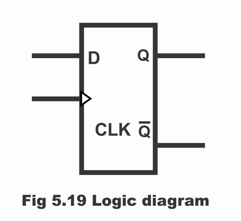
- When clock is high or 1, in such a situation flip-flop does not operate as well, as a result no change occurs on output (see line number 2 of the table)
- When clock is on the negative edge, in such a situation too flip-flop remans disabled. Resultantly, output does not change at all (see truth table line number 3)
- When positive going clock edge appears, in such a condition flip-flop enables or activates due to a zero-binary value (i.e. D = 0). Thus, input data transfers on output Q (i.e. both D and Q has same value). Here as the value of D is zero, therefore value of Q also becomes zero (i.e. flip-flop resets). However, according to definition of a flip-flop, value of complement output Q equals to 1 (i.e. Q = 0 and Q = 1) as can be seen via line 4 of the truth table. In other words, if clock pulse is applied and D input is low, flip-flop tends to reset. Thus, input D stores on leading edge or negative edge of clock pulse to be received on output. Remember that in reset state, flip-flop stores 0.
- When positive going clock edge appears, then in situation of data input being equal to 1, flip-flop enables and transfers D’s value on Q (i.e. D = Q), in this way flip-flop sets. In other words, when clock pulse is applied in case of a high D input, flip-flop sets. Thus, D input stored on positive going edge of the clock pulse, is received on to the flip-flop output. Remember that in a set state, flip-flop stores 1. As both set and reset states of a positive edge triggered D flip-flops are very important, therefore for simplicity purposes, both these states have been shown in figure 5.20.
Figure 5.20 – truth table for positive edge–triggered D flip-flop
| Inputs
D CLK |
Outputs
Q Q |
Comments |
| 1 ↑
0 ↑ |
1 0
0 1 |
SET (stores a 1)
RESET (stores a 0) |
Preset and Clear Facility
Commercially available D flip-flops are predominantly manufactured in an IC shape, along with two additional inputs preset and clear, also included. In figure 5.21, a logic circuit of D flip-flop containing preset and clear features, has been shown while in figure (a) logic symbol of a commercial D flip – flop and in figure (b) its truth table has been illustrated. In the logic symbol, preset input has been denoted by PS and clear input represented as CLR. When PS input is enabled via logic 0, it sets output Q on 1, whereas when CLR is enabled through logic zero, it brings output Q to zero (i.e. output Q becomes clear or reset). This has been illustrated vide line 1 and 2 of the table. These PS and CLR inputs (or asynchronous inputs) repudiates D and CLK inputs (or synchronous inputs). This state has been reflected via X through the table. However, D and CLK inputs operate here as well in a usual manner just similar to the way they operate in a D flip-flop. The first three lines of the truth table have been explaining the operation or working of D flip-flop controlled asynchronous inputs. The prohibited state as has been displayed vide line number 3 of the truth table, must inevitably be avoided (i.e. flip-flop must never be operated on such a state because this state is totally contrary to the basic definition of a flip-flop). When asynchronous inputs are disabled, or when they do not operate, (i.e. PS = 1 and CLR = 1), in such a situation, D flip-flop can be set or reset by means of using D and CLR inputs. This can be seen from the last two lines of the truth table. In these two lines, flip-flop input data D has been illustrated having been transferred on output Q by means of using a clock pulse. Such an operation of data transfer by means of a clock, is called synchronous operation.
Figure 5.21 – edge-triggered D flip-flop with preset and clear
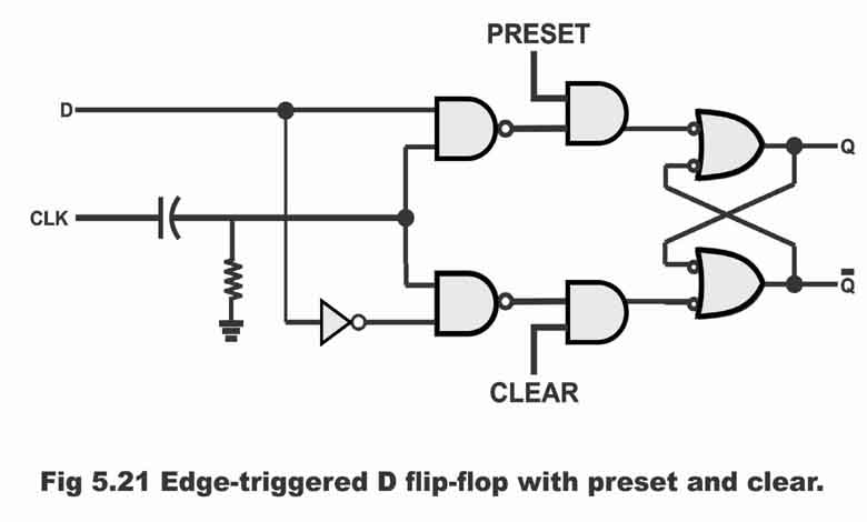
Figure 5.22 – (a). logic symbol for a commercial flip-flop (b). truth table for 7474 D flip-flop
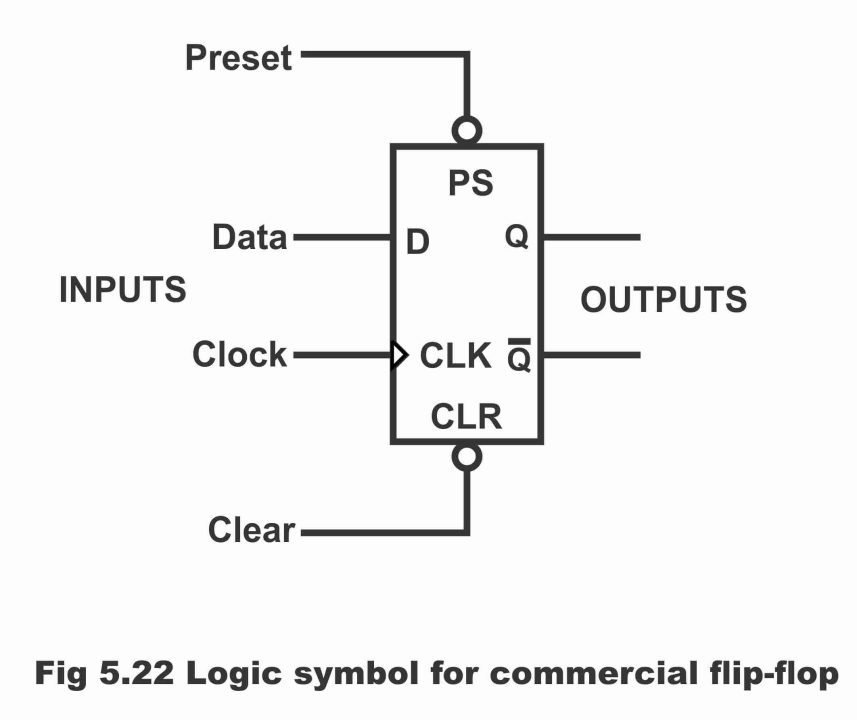
Remember that when PS and CLR both are low, race condition builds up, i.e. both outputs become high simultaneously (this state has not been reflected in the table) thus, when PS and CLK are not being operated, they have to be high. Moreover, output changes only on positive going edge of the clock.
D flip-flops are sequential logic devices which are extensively used as transitory memory devices. D flip-flips are wired or interconnected in order to manufacture shift registers as well as storage registers. These registers are commonly used in digital systems. D flip-flops are available both in TTL – IC, and CMOS – IC form. 74HC74, 74AC74, 74FCT374, 74HC273, 74AC273, 4013, and 40174 are some of the famous CMOS D flip-flops, which are quite popular.
Previous Topic: RS Flip-flop Circuits using NAND Gates and NOR Gates
Next Topic: JK Flip-flop: Positive Edge Triggered and Negative Edge-Triggered Flip-Flop
For electronics and programming-related projects visit my YouTube channel.
Discover more from Electronic Clinic
Subscribe to get the latest posts sent to your email.