RS Flip-flop Circuits using NAND Gates and NOR Gates
Last Updated on August 3, 2025 by Engr. Shahzada Fahad
Table of Contents
RS Flip-flop
RS Flip-flop (or Reset – set flip-flop) is the simplest of all flip-flops. This basic type of flip-flop is also called direct – coupled flip-flop or a latched flip-flop. Remember that as a flip-flop has two possible stable states (precisely analogous to a toggle switch which can either turn ON or OFF) and remains on its stable state or hold its one particular state until its input changes and as such, forcefully changes its hold position. This holding feature is known as a latch, due to which a RS flip-flop is also known as a latch flip-flop. A flip-flop has two inputs R and S (here S means set whereas R means reset). S input is used in order to get a flip-flop set, while R input is used to reset this flip-flop. In case of a set flip-flop, it stores binary 1, while in case of reset, the flip-flop stores binary 0. It must be inculcated into mind that when logic signal is applied on flip-flop inputs, the flip-flop (latch) then changes its state. A RS flip-flop comprises two outputs Q and Q apart from two inputs R and S (Q is known as Q not or Q bar). In order to denote a flip-flop state, its output has always been taken into consideration or looked upon principally. Here Q means normal output, whereas Q means complementary output (or output precisely opposite to normal output) as has been illustrated vide a logic symbol of an RS flip-flop in figure 5.2. in other words, both outputs of a RS flip-flop are exactly opponent of each other.
Figure 5.2 – logic symbol for an RS flip-flop
Figure 5.3 – Truth table for an RS Flip-flop
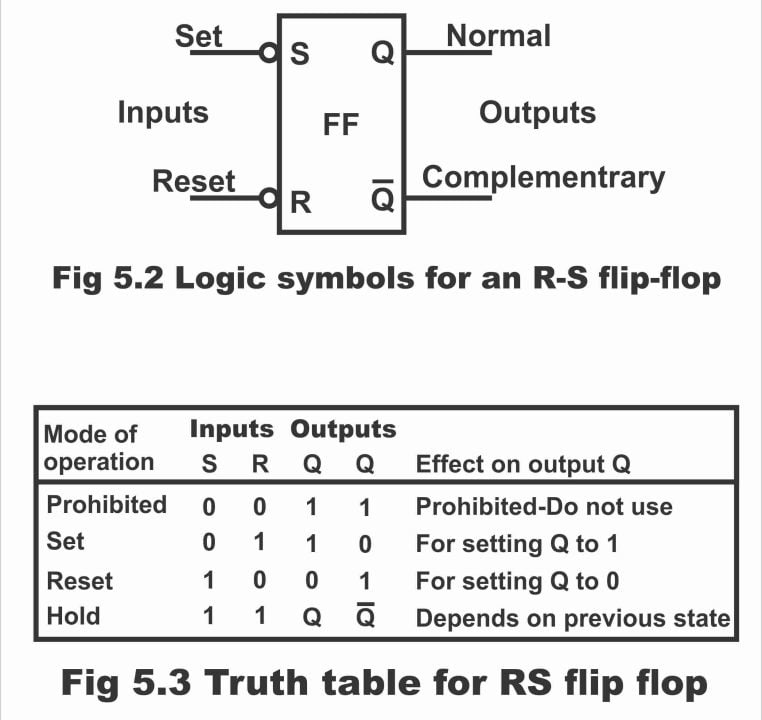
| Mode of Operation | Inputs
S R |
Outputs
Q Q |
Effects on Output |
| Prohibited | 0 0 | 1 1 | Prohibited – Do not use |
| Set | 0 1 | 1 0 | For setting Q ro 1 |
| Reset | 1 0 | 0 1 | For resetting Q to 0 |
| Hold | 1 1 | Q Q | Depends on the previous state |
The truth table displayed in figure 5.3 explains the operation of an RS flip-flop, according to which;
- When S and R both inputs are 0, in such a situation, both outputs are logical 1. This state is known as prohibited state and this state is not used (i.e. for normal flip-flop operation, both of its inputs are never brought to binary 0)
- When value of input S is 0 and value of input R is 1 (as has been shown on line 2 of the truth table, under such a situation Q output sets on logical 1 and such a state of flip-flop is called set condition.
- When value of input R is 0 and value of input S is 1 (as can be seen in the 3rd line of the truth table) in such a case, output Q becomes reset or 0. This is known as reset condition.
- When both inputs S and R are 1 (as shown in line 4 of the truth table) in such a situation both outputs (Q and Q) retreat to their previous complementary state or in other words flip-flop holds or sustains on to its previous state. This state of flip-flop is known as an idle condition or at reset condition or hold condition.
If truth table is studied further deeply, it becomes obvious that in order to activate it on set (i.e. setting Q on 1) also necessarily requires logical 0. As a flip-flop necessitates logic 0 in order to enable or activate it, therefore reversed bubbles have been drawn above R and S inputs as has been illustrated via RS flip-flop’s logic symbol in figure 5.2. The bubbles indicate that both set and reset inputs of the flip-flop is activated by means of logical 0.
A basic RS flip-flop circuit can be fabricated with the help of two NAND gates or two NOR gates. Both reversed gates (NAND & NOR) existing on the circuit are crossed–coupled reciprocally i.e. output of one gate is input of the other gate. Thus, a feedback path develops due to which such flip-flop circuits are called asynchronous sequential circuits. Remember that other complicated flip-flop circuits can also be constructed with the help of a basic flip-flop circuit.
The explanation of RS flip-flop or latch circuits manufactured through NAND and NOR gates, has been given as follows:
RS Flip-Flop Circuit with NAND Gates
In figure 5.5 (a), a basic RS flip-flop circuit consisting of two NAND gates and in figure (b) its truth table has been depicted. It must be remembered regarding NAND gate mechanism that when both of its inputs are on 1, its output becomes zero (i.e. its output state changes) and as result of any one or both inputs being on zero or low, NAND gates’ output becomes 1 or high.
Figure 5.5(a). wiring an R-S flip-flop using NAND gate
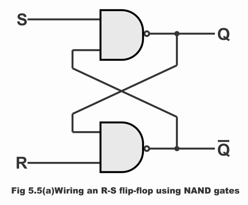
Operation
The operational mechanism of a basic flip-flop circuit, comprising a NAND gate is as follows:
Figure 5.4 (b) – truth table for NAND gates RS flip-flop
| Inputs | Outputs | ||||
| Mode of operation | S | R | Q | Q | Effect on output |
| Prohibited | 0 | 0 | 1 | 1 | Prohibited or forbidden (do not use) |
| Set | 0 | 1 | 1 | 0 | Set to 1 |
| Reset | 1 | 0 | 0 | 1 | Set to 0 (clear state) |
| Hold | 1 | 1 | Q | Q | Previous or last state (no change) |
(i). When both inputs are 0, then both outputs become 1. This state is called forbidden or a prohibited condition. Flip-flop is never made to act in this state during normal operation, as has been illustrated in the truth table.
(ii). According to second line of the truth table, when S input is 0 while R input is 1, then in such a situation, output Q becomes logic 1 and output Q becomes logic 0. Consequently, flip-flop pass on to a set condition (i.e. it sets on 1)
(iii). When S input is 1 and R input is 0, output Q becomes reset (i.e. it sets on zero). This condition is also known as clear state, as has been illustrated vide line 3 of the truth table.
(iv). When both inputs are 1, in such a situation both outputs retreat on to its previous or last condition. Resultantly, no change substantiates. This condition of any flip-flop is known as a hold condition. It has been exemplified through line number 4 of the truth table.
Alternative Explanation
According to truth table, the operational mechanism of an RS flip-flop or latch flip-flop can also be explained as below:
Suppose that value of Q is 0 (i.e. Q = 0) and value of R is 1 (i.e. R = 1). As output Q is also input of the bottom gate, in such a situation one input of the bottom gate (which is associated with Q) is 0 while other input (which is associated with R) is 1. We know that output of a NAND gate becomes 1 in case any one of its inputs is 0. Thus, in such a situation, output of the bottom gate turns out to be 1 (i.e. value of Q becomes 1 which is converse or complement of Q). As Q output is also input of the top gate, and if S input of top gate is 1 (i.e. S = 1), then output of this particular gate becomes zero (i.e. Q = 0) as a result of both inputs of top gate being 1. It means that 0 value of top gate’s Q output, keeps the bottom gate continuously disabled (i.e. prevents it from any sort of operation), so that there is no influence whatsoever of any sort of a change in R. similarly, a state 1 on Q, keeps top gate persistently enabled, thus any change taking place in S, will be transmitted on to Q. As the value of Q remains 0 throughout this process, therefore this condition of the device reflects a stable state i.e. Re – set state, which has been demonstrated by line number 3 of the truth table.
Now presume that RS flip-flop is in a re-set state and value of S input becomes 0. Under such a situation, output Q of the top gate becomes high or 1 (owing to any one of the two inputs being 0 or low). As Q output also happens to be input of the bottom gate, thus due to inputs of both the bottom gate being high (i.e. Q = 1 and R = 1) output Q of the gate becomes 0. As output of the bottom gate is also input of the top gate, therefore top gate remains disabled (or it does not operate), therefore its output Q remains set on 1. Resultantly, when value of S is 1, under such circumstances there is no influence on flip-flop as well (because in case any one or both top gate inputs being zero, its output Q remains 1 or high). Whereas, as a result of change in R, output of bottom gate will also change. This operation of a flip-flop describes an alternative stable state which is known as a set–state. It is because of the fact that value of Q remains 1 in this state, which has been illustrated vide line number 2 of the table. Remember when state of S modifies from 1 to 0, the flip-flop shifts from a re–set state to a set state.
When both of the inputs R and S are on logic state 0, both outputs Q and Q raise high or become 1 and they remain on this state as long as values of R and S remain zero. When both inputs become 1 there is no source to determine whether a flip-flop retains or latches to a set state or latches on to a reset state. This state is known as indeterminate state or holding condition.
RS Flip-flop Circuit with NOR Gates
In figure 5.5 (a) an RS flip-flop containing two NOR gates and in figure (b) truth table of NOR gate RS flip-flop has been illustrated. It should be remembered about NOR gate that its output is 1 only when all of its inputs are 0. And when any one or both of the NOR gate’s inputs are 1, its output is 0.
Figure 5.5 – RS latch flip-flop using NOR gate
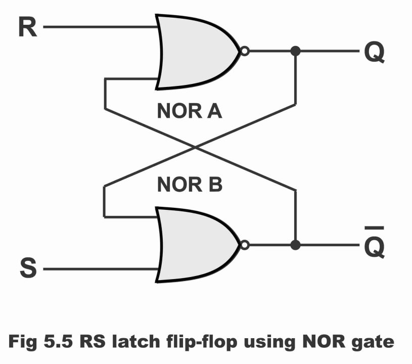
Figure 5.5 (b) – Truth table for a NOR – gate RS flip-flop
Operation
(i). When both inputs are 0 (i.e. R = 0 and S = 0) in this situation NOR gates inputs have no influence whatsoever on its output as long as input condition of flip-flop does not change. As such, flip-flop remains on its present or normal state i.e. no change occurs in the value of Q, which has been illustrated by the 1st line of its truth table. Remember that if S input becomes 1 for a moment, flip-flop moves on the set state. Similarly, if R input goes 1 for a moment, in such a situation flip-flop shifts to the reset state or a clear state.
(ii). When value of R is 0 and value of S is 1 (i.e. R = 0 and S = 1), in such a situation, output of the bottom NOR gate becomes 0 or low. As output of bottom gate is also an input of the top gate, in this way both inputs of the top gate become 0 or low. Resultantly, output of the top gate becomes high or 1. As such, flip-flop sets when input S becomes 1. Remember that when flip-flop output Q is 1 (i.e. Q = 1), this stable state of flip-flop is called set. This has been demonstrated vide 2nd line of the truth table.
(iii). When R input is 1 and S input is 0 (i.e. R = 1 and S = 0) the output value of top NOR gate becomes 0 or low. As output of top gate is an input of the bottom gate, hence both inputs of the bottom gate become zero or low. As a result, high output is obtained from bottom gate. Therefore, applying 1 on R input, flip-flop resets on a stable state (where Q = 0 and Q = 1), which is known as a clear state or reset state
(iv). When both inputs are 1 (i.e. R = 1 and S = 1), a forbidden state prevails on flip-flop. As a result, outputs of both NOR gates become 0 or low. In other words, values of Q and Q become identical or same (i.e. Q = 0 and Q = 0). As this thing is absolutely opposite to the rudimentary definition of a flip-flop (remember that as per basic definition of a flip-flop, both outputs of a flip-flop are commonly inverted or opposite), therefore under normal circumstances, both flip-flop inputs do not become 1 simultaneously. If such a situation arises fortuitously, state of output Q becomes indeterminate or indescribable. This condition is occasionally, represented in a truth table by a question mark.
Clocked RS Flip-flop
An RS flip-flop which consists of a 3rd input as well, instead of a set and reset inputs which are known as a clocked input, is called a clocked RS flip-flop. In other words, a clocked RS flip-flop practically resembles an RS flip-flop, with the only exception that an additional input CLK (which is called clock input) is being applied to it and on account of this particular reason, it is termed as a clocked RS flip-flop. Remember that a clocked RS flip-flop’ s output changes as a result of a change in clock’s inputs. That’s clock inputs of such type of a flip-flop controls its output, due to which it is also known as a clock input control pin. Clocked RS flip-flop is also known as Gated RS flip-flop. This is an important flip-flop circuit, because all other flip-flops are manufactured through it.
In figure 5.6 (a), wiring or logical diagram of a NAND- gates clocked RS flip-flop, in figure (b) logical symbol along with its timing diagram and in figure (c) truth table of clocked RS flip-flop has been illustrated. As can be seen in figure (a), a clocked RS flip-flop consists of one basic flip-flop circuit and two additional NAND gates. As such, it has overall three inputs i.e. set input, reset input and clock (CLK) input or enabled input. Here, CLK input behaves as an enabled signal for other two inputs (i.e. this flip-flop changes its condition only when a clock pulse is also applied along with an input variation). For example, when clock pulse or clock input is 1, flip-flop output tends to change. In other words, data existing on flip-flop input shifts on output. However, when clock input is zero, flip-flop output remains on its previous state no matter whatever the values of R and S inputs (i.e. no change reflects on output). In other words, when clock input or enable input (which is shortly written as EN) is low, no impact can be witnessed on flip-flop Q output in spite of changes in R and S. This condition of a latch is called disabled. On the contrary, when clock or enable input is high, all information available on R and S inputs, transmits directly on output. This condition of RS flip-flop or latch is known as enabled. As such, output continue to change as long as clock input remains high besides changes in the flip-flop inputs.
Figure 5.6 (a) – clocked RS flip-flop
Figure 5.6 (b) – logic symbol with timing diagram which show how the Q output responds to R, S and CLK inputs
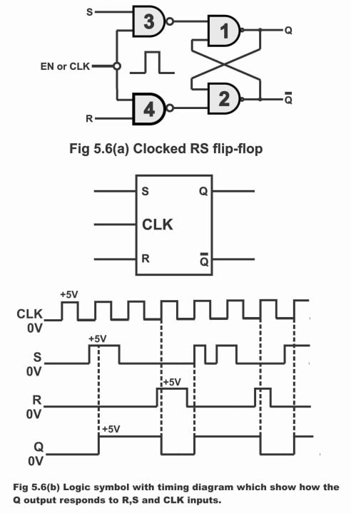
Figure 5.6 – Truth Table
| CLK | R | S | Q |
| 0 | 0 | 0 | NC |
| 0 | 0 | 1 | NC |
| 0 | 1 | 0 | NC |
| 0 | 1 | 1 | NC |
| 1 | 0 | 0 | NC |
| 1 | 0 | 1 | 1 |
| 1 | 1 | 1 | Illegal* |
As soon as enable or clock input turn out to be low, the information which has been available on flip-flop’s output when the clock input was high, that information is still accessible even when the clock input turn from high to low (i.e. flip-flop survives on to its previous condition during this operation). In this way, it seems possible to set or re-set a flip-flop any time and hold stored data or information intact up to a desired time limit.
Operation
According to truth table shown in figure 5.6 ©, a clocked RS flip-flop operates in the following manner.
(1). When clock input is zero or low, then irrespective of the values of R and S inputs (i.e. 00, 01, 10 or 11) no change ensues on flip-flop output Q (or there is no impact on the output). This has been revealed via first four lines of the truth table. As in such a situation, as long as clock input remains on 0, NAND gate 3 and 4 outputs stick to the logical level 1. Here, output Q has been represented as NC (which means a no change)
(2). When clock input is high or 1, while other two inputs are low or 0, no change will happen in output either. This has been reflected vide line 5 of the truth table.
(3). When clock (CLK) input is high, whereas R value is 0 and value of S is 1 (i.e. CLK = 1, R = 0 and S = 1), in such a situation, flip-flop tends to set (i.e. flip-flop output Q turns out to be high or 1) owing to gate number 3 output being 0 but gate number 4 output being 1. This has been illustrated vide line No. 6 of the truth table.
(4). When clock input is high and R value is 1, while S value is 0 (i.e. CLK = 1, R = 1 and S = 0), then owing to a 0 gate No. 4 output but a 1 output on gate No. 3, flip-flop resets (i.e. its output Q becomes zero). This has been demonstrated on line 7 of the truth table. Once a flip-flop has been set or re–set, it retains its last stable state even if R and S inputs values become 0 or low.
(5). When all inputs are high or 1 (i.e. CLK = 1, R = 1 and S = 1), according to definition this condition of a flip-flop turns out to be illegal or indeterminate or prohibited. This has been illustrated in the final line of the table. This is because in such a situation, outputs of both gate numbers 3 and 4 tend to be 0 or low, resultantly both output values Q and Q turns out to be 1 concurrently. Remember that according to the flip-flop definition, values of both Q and Q are inverted or opposed together, however practically this state is never being used.
It must also be kept in mind that thousands of flips–flops are used in computers. In order harmonize the operations of different flip-flop circuits being used in a computer system, every flip-flop is transmitted a clock signal. This clock input signal, thwarts flip-flop outputs from undergoing any sort of changes at different times. And allows outputs to be changed only at the designated correct time.
Alternative Explanation of Clocked RS Flip-flop
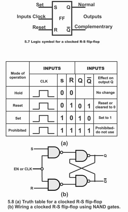
A rudimentary RS flip-flop circuit, which apart from set and reset inputs also consists on an additional (CLK) or enable storage, is known as clocked RS flip-flop (i.e. clocked RS flip-flop consists of three inputs, set input, reset input and clock input). It must also be inculcated that clock inputs introduced on a clocked RS flip-flop control output of this particular flip-flop. This is the reason; a clocked input is also sometimes known as control pin. When clock input is 1, in this situation information available on a flip-flop input, transmits on to its output. However, when clock input is zero, whatever the values of R and S, no change occurs on flip-flop‘s output. In other words, flip-flop output retains on its previous state.
In figure 5.7, logic symbol of a clocked RS flip-flop and in figure 5.8 wiring of clocked RS flip-flop (wherein NAND gates are used) have been shown along with corresponding truth table. As per logic diagram or wiring diagram, this flip-flop consists of three inputs (R, CLK, S) and two outputs (Q and Q), as has been shown via diagram. If wiring diagram is warily studied, it becomes obvious that this clocked RS flip-flop has fundamentally been constructed on input side of the flip-flop’s circuit by means of mounting two NAND gates and making one of each these NAND gates’ input common, a clock (CLK) pulse is provided on to it.
Figure 5.7 – logic symbol for a clocked RS flip-flop
Figure 5.8 – (a) truth table for a clocked RS flip-flop (b). wiring a clocked RS flip-flop using NAND gates
Operation
According to truth table as shown in 5.8 a clocked RS flip-flop operates as follows:
- When clocked input is high or 1, and other two inputs R and S are low or zero (i.e. R = 0, S = 0 and CLK = 1), in such a situation, there is no impact on output Q or that no change occurs in output Q. This has been explained vide line No. 1 of the truth table. This condition is generally referred to as “Hold”, because in such a situation, flip-flop holds on to its previous state or stick to its last state.
- When clocked input is 1, value of S is zero while that of R input is 1 (i.e. CLK = 1, S = 0 and R = 1), in this case value of output Q turns zero while output Q turns out to be 1. In other words, in such a situation, flip-flop tends to reset, owing to which output Q becomes zero. This has been demonstrated via line 2 of the truth table.
- When clocked input is 1, value of S input 1 and value of R input is 0 (i.e. CLK = 1, S = 1 and R = 0), in such a situation value of output Q turns out to be 1 whereas value of Q becomes zero. In other words, flip-flops set in this case, by means of which its output becomes 1. This has been exemplified vide line No. 3 of the truth table.
- When all inputs along with clocked input become 1 (i.e. CLK = 1, S = 1 and R = 1) then in such a case, both flip-flops outputs (Q and Q) turn to 1 instead of being reversed together. In this way, a prohibited state develops on the device, as can be seen from the last line of the truth table. However, practically, this state is not being used at all.
- When clocked input is zero, whatever the values of R and S inputs (i.e. 00, 01, 10, 11) no change happens in flip-flops’ output Q. This is because clocked RS flip-flop’s output always changes by means of a clocked pulse. Therefore, 0 clocked pulse state has been ignored in the truth table.
In figure 5.9, this operation of clocked RS flip-flop has been illustrated with the help of a diagram or a timing diagram. In this figure, clock input (CLK) has been depicted on topmost portion. After studying the figure, it becomes evident that when values of R and S inputs are 0, at that time clock pulse 1 has no effect whatsoever on Q output. As a result, flip-flop remains in an idle or hold condition during clock pulse 1. This has been illustrated in the first line of the truth table.
Figure 5.9 – waveform diagram for a clocked RS flip-flop
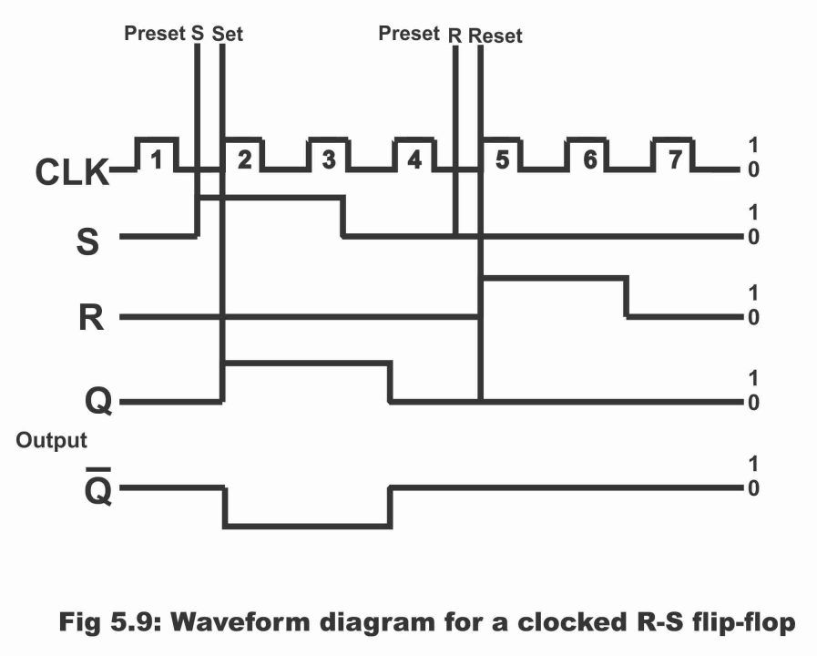
The value of input S becomes 1 on preset position S, however output Q cannot be set at 1 owing to a 0 clocked pulse. However, when clock pulse turns to 2, at that time value of S is already 1, whereas value of R is 0. Therefore, flip-flop sets immediately and value of its output Q becomes 1. This can be seen vide line 3 of the truth table. After this, clock pulses 3 and 4 have no impact whatsoever on output Q because flip-flop tends to remain in its set – mode during clock pulse 3. Whereas in case of clock pulse 4, it remains in its hold mode (i.e. remains on its last or previous condition), as the value of set input S has already turned on 0 prior to the advent of clock pulse 4.
Afterwards, input R enters into a preset state whereas the value of input S at that time is 0. In such a condition, flip-flop resets as a result of arrival of clock pulse 5 or due to its having been high. As a result, output Q turns out to be zero, which has been demonstrated through line No. 2 of the truth table. Afterwards, flip-flop remains in a reset state during both clock pulses 5 and 6. However during the clock pulse 7, flip-flop enters into a hold mode (i.e. it holds or retains on to its previous condition or subsists on a state of 1 value of output Q or output Q)
It must be inculcated into mind that outputs of a clocked RS flip-flop changes only as a result of clock pulse, therefore we may say that this flip-flop operates synchronously (i.e. it works along clock or when clock value becomes 1). In calculators and computers etc., where each step or action has to be properly and precisely configured, synchronous operation has a paramount significance. Another important feature of a clocked RS flip-flop is that once it has been set or reset, it continues to remain on its present condition despite changes in its inputs. This particular memory characteristic of this flip-flop has an incredible importance in numerous digital circuits. It has to be remembered that this feature of the device is retained even during a hold mode.
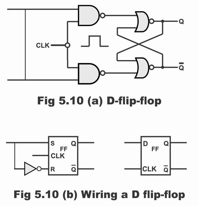
Figure 5.10 – (a) D flip-flop
Previous Topic: Flip-Flop Combinational logic circuits and Sequential logic circuits
Next Topic: RS Flip-flop Circuits using NAND Gates and NOR Gates
For electronics and programming-related projects visit my YouTube channel.
Discover more from Electronic Clinic
Subscribe to get the latest posts sent to your email.