Logic AND Gate Working Principle & Circuit Diagram
Last Updated on March 6, 2024 by Engr. Shahzada Fahad
Table of Contents
The AND Gate
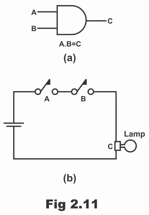
The AND gate is a digital circuit that consists on two or more than two inputs and just one output. As a result of any low input of this gate, low output is received. And when all inputs of this gate are high, a high output is received. That’s the reason AND gate is also known as “all or nothing” gate. i.e. any input is zero, output is zero. In figure 2.11, electronic or logic symbol of AND gate has been illustrated. In figure b, its equivalent switching circuit has been shown. On the left side of AND gate symbol, two inputs A and B and on the right side one output C can be seen. It must be remembered that value three variables A, B and C can either be zero or 1. Output of AND gate is 1 only both its inputs are at level 1.
Logic Operation of the AND Gate:
- Output is obtained from the AND gate only when all of its inputs are available.
- When any one input of all the NAND gate’s inputs is zero or low, the resulting output will also be low.
- Output of AND gate is high or 1 only when the inputs level of both A and B is high or 1.
- If the term True or False is used instead of high or low (i.e. 0 or 1), the output of AND gate will be true only when all of its inputs are True. Conversely, in case any one of its inputs is false, the resulting output will also be false.
- As such, AND gate just functions like a bulb and two switches fitted on a series (that’s as a series switching circuit). Here bulb reveals output whereas two switches represent the output. As can be seen from an equivalent switching circuit to the AND gate as shown in figure (b). Bulb radiates or enlightens only when both switches (A and B) are on or close. If any one of the two switches is opened or off, the bulb does not illuminate.
The logical operation of an AND gate can easily be understood via the below figure

Boolean Expression of the AND Gate:
In the case of logic expression or Boolean algebraic form of AND gate, it can be written in the arithmetic form as follows:
0.00 = 0
0.1 = 0
1.0 = 0
1.1 = 1
If one of the inputs is variable A and other input variable B, whereas C is output variable, then in case of equivalent expression, it can be mentioned as follows (remember that variable on each input can either be 0 or 1).
A.B = C
Or A x B = C
Or AB = C
The dot or multiplication symbol in this Boolean algebraic expression represents AND. i.e. A & B are equal to C. The dot or multiplication symbol in these equivalent expressions reflects logical multiplication, which is different from arithmetic multiplication. According to logical multiplication, the meaning of above equation/expressions is as follows:
- Output C is 1 only when the value of each of the two inputs A and B is 1
- Output C is True only when both inputs A and B are True
These two points may also be explained with the help of an equivalent switching circuit as shown in figure 2.11 (b). that’s lamp radiates or becomes ON only when both the switches A and B are close. Otherwise, the lamp remains OFF in case any one of these two switches is open.
Figure 2.13 (a) 2-input AND gate
| A | B | C |
| L | L | L |
| L | H | L |
| H | L | L |
| H | H | H |
Figure 2.13 (b)
| A | B | C |
| 0 | 0 | 0 |
| 0 | 1 | 0 |
| 1 | 0 | 0 |
| 1 | 1 | 1 |
Truth tables are drawn through Boolean algebra as follows:
| A x B = C
0 x 0 = 0 0 x 1 = 0 1 x 0 = 0 1 x 1 = 1 |
Diode AND Gate
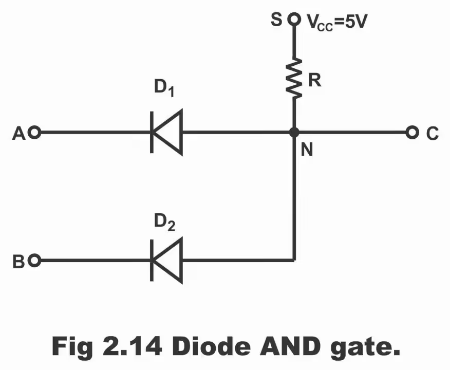
In figure 2.14, a diode AND gate circuit has been shown which consists on two inputs A and B. The logical operation of this AND gate made from two diodes, is as follows:
- When the value of A is zero, the diode D1 conducts and a drop of +5V supply voltage occurs parallel to R. Resultantly, the value of point N and point C becomes 0V (or potential of point N and point C becomes zero volt), therefore output received on C also becomes zero. In other words, when input A is on zero level, the top diode D1 becomes forward biased and starts conducting. In such a situation, diode on the bottom end becomes reverse biased as a result of its high input. Resultantly, point C and point N become grounded due to conducting of D1 (that’s the level of these points becomes zero)
- Similarly, when the value of input B is zero volt, the diode D2 conducts where diode D1 remains off due to being reverse biased. In this way, point N becomes grounded. As a consequence, the value of output C becomes zero volt. In other words, when input B is at zero level, out C also remains on zero level.
- When the value of both inputs A and B is zero volt, in such a situation, both diodes D1 and D2 conduct and then the value of output C becomes zero. That’s low output is achieved as a result of both low inputs.
- When value of both the inputs A and B is +5V, the potential of both inputs and supply point is equal, due to which diodes do not conduct (because there are zero volts parallel to each) and no supply current passes through R. Thus, no voltage drop takes place parallel to R. in such a situation, +5V are received on output C. In other words, when both of the inputs are high (i.e. +5V or level 1), both the diodes do not conduct (that’s they remain off). Therefore, a high output is received (i.e. +5V are received on point N and point C or the level of both points become 1)
Figure 2.14 – Diode AND gate
Three-Input Diode AND Gate
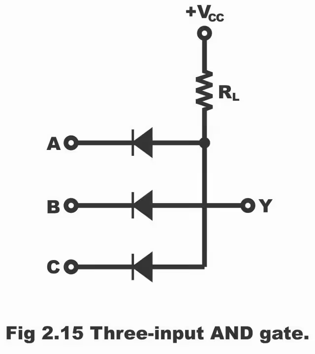
In figure 2.15, an AND gate comprising three inputs has been shown. When all inputs are low, all diodes conduct, owing to which a low output is obtained. Even if one of the inputs is low, the output will be on low state, because diode connected with low input does not conduct. There is just one way of getting a high output from this type of a gate and it is to bring all inputs on +5V. when all inputs are high, none of the diodes conduct, thus supply voltage +5V are received on output. In the figure 2.16, truth table of a three inputs AND gate has been shown. Remember that the number of rows in any truth table is always equal to 2n, here means number of inputs. For example, in case of two inputs, 4 rows are there in a truth table (i.e. 22 = 4), similarly truth table consisting three inputs, is made up of eight rows i.e. 23 = 8.
Figure 215 – Three -input AND gate Figure 2.16
Transistor AND Gate
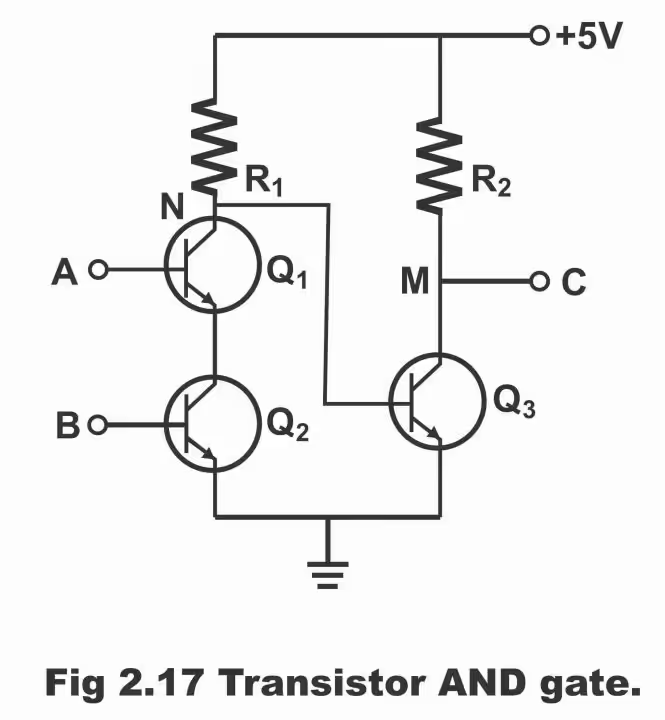
In the figure 2.17, a transistor AND circuit has been depicted, which consists on two inputs A and B and one output C. when both inputs A and B are at +5V, both the transistors Q1 and Q2 conduct (suppose in saturation region). Thus, the current which is produced, passes through R1 and drops the supply voltage +5V parallel to R1. Therefore, point becomes grounded (i.e. its potential becomes zero). As point N is connected to the base of Q3, therefore Q3 also becomes grounded by virtue of N being ground. Resultantly, Q3 gets cut – off, thus supply voltages equal to +5V are received on output point C.
If there is zero volt on any one of either A or B (that’s on the base of Q1 or Q2), then Q1 or Q2 will cut – off and no drop will occur parallel to R1, thus +5V are received on point N, by means of Q3 starts conducting (because Q3 base is connected to point N) and the whole supply voltages will drop parallel to R2. As such zero voltages will be received on point M and output C or output C will become grounded.
Figure 2.17 – transistor AND gate
Previous Topic: Introduction to Logic Gate with Examples
Next Topic: Logic OR Gate Working Principle & Circuit Diagram
For electronics and programming-related projects visit my YouTube channel.
Discover more from Electronic Clinic
Subscribe to get the latest posts sent to your email.
