Logic OR Gate Working Principle & Circuit Diagram
Last Updated on September 17, 2022 by Engr. Shahzada Fahad
Table of Contents
The OR Gate
A gate which consists on two or more than two inputs (or input signals) and only one output (or output signal) and which results in a high output in case any one or all the inputs on the gate are high, is known as OR gate. As output voltages of OR gate tend to become high by means of high voltages of either one input or all the inputs on gate, therefore OR gate is also occasionally known as “any or all gate”.
Any input is one (high), output is one (high)
The standard logic or electronic symbol of a OR gate comprising two inputs has been illustrated via figure 2.4 (a) its equivalent switching circuit by figure (b), whereas truth table of OR gate has been depicted by figure (c). (Remember that a table which reflects all input – output possibilities of any digital circuit, is known as truth table or a table which describes output levels or states of any logic device with respect to its inputs, is called truth table. That’s to say output resulting from entire facts pertinent to inputs, are based on some kind of a truth, that’s why this type of arithmetic table is known as a truth table)
Figure 2.4
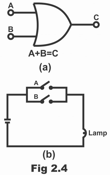
In the figure, both inputs have been shown by A and B whereas output has been presented by C. it is worth mentioning here that according to Boolean algebra, the value of all three variable i.e. A, B and C could be between 0 to 1.
Logic Operation
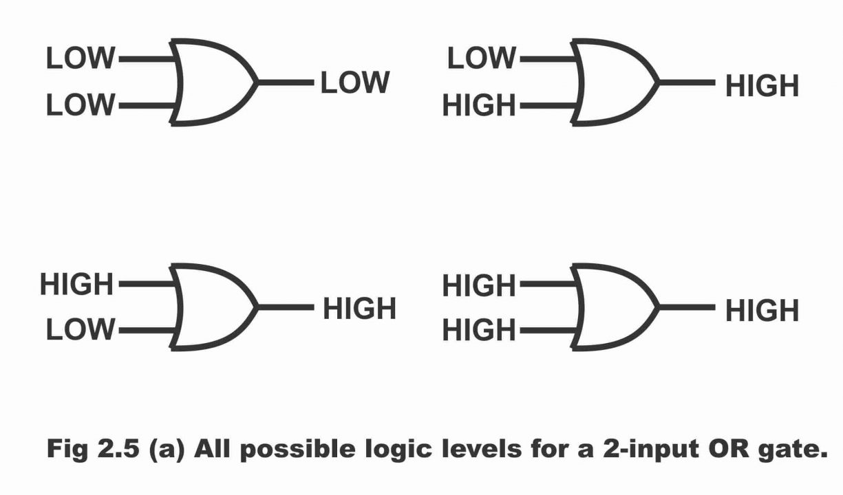
We know that output of OR gate is 1 or high at a time when any one of its inputs (i.e. A or B) or both inputs are 1 or high. In other words, OR gate is such a “any or all” gate, wherein output is 1 or high in case any one or both of its inputs are 1 or high. (The logic operation of an OR gate can also be explained via figure 2.5 “a”). As such, this gate operates like two switches fixed parallel to a lamp, as can be seen through figure 2.4 “b”. When any one of these switches (A or B) or both switches (A or B) are closed or turned ON, the lamp irradiates (logic 1) by means of getting battery voltages. However, on the contrary, if both switches (A or B) are kept OFF or open (that’s both inputs are 0) the lamp will remain OFF (logic 0), or it will not illuminate (i.e. output will be zero, as can be seen in the OR gate’s truth table).
Figure 2.5 (a). all possible logic levels for a 2-input OR gate
Boolean Expression
OR gate can be presented by means of following Boolean expression (remember that in algebraic language, (+) sign is used for OR and it is different from Boolean addition or binary addition)
| A+B=C |
The meaning of this equation is that output C is high at a time, when either of inputs (A or B) or both inputs A and B are high. (This point can easily be explained through a truth table shown in figure 2.5 “b”). In other words, this equation implies that output C is 1 at a time when either input A or input B or both of the inputs A and B are high.
| Truth Table of Two Input OR Gate | ||
| A | B | C |
| Low | Low | Low |
| Low | High | High |
| High | Low | High |
| High | High | High |
Figure 2.5
Truth Table: As this gate has two inputs, therefore it is likely to have four possible states or positions i.e. 00, 01, 10, 11. Further, value of C can be determined by means of inserting different values of A and B in this equation.
Explanation of truth table is as under:
- When both inputs are zero or low (due to switches being open), output is zero or low (i.e. lamp remains off)
- When input A is zero or low that’s on logic state 0 (in case of an open switch A) and input B is on logic state 1 or high (in situation of a closed switch B), the output C is at logic state-1 or high (i.e. lamp turns on).
- When input A is high or 1 (on close of switch A) and input B is zero or low (on switch B being open), then output C is high or 1. In such a situation too, lamp tends to illuminate.
- When both inputs are 1 or high, or when both switches are closed, even then output is 1 or high and the lamp tends to radiate. As such, OR gate is equivalent to a parallel circuit by means of its logic function.
Diode OR Gate
In order to understand the function of OR gate, if two diodes are used instead of two parallel switches, such a circuit is known as diode OR gate. In figure 2.6, a diode OR gate has been illustrated consisting of two typical input diodes D1 and D2 parallel to output C. The working details of which are as under:
- When there is +5V on A, D1 conducts due to being forward biased. As such, circuit current flows via resistor R and a 5V drop occurs across R. In this way, +5V are obtained on point C (or output). In other words, when input A is high and input B low, in such a situation, diode on the top D1 conducts (or turns on) whereas the bottom diode D2 remains off. In this way, an ideal +5V or high output is received parallel to the resistor (it has to be remembered that practically, in case the diodes’ voltage is also included, then +4.3V will actually be received on output)
When +5V are provided on input B, diode D2 conducts, while diode D1 remains off. Thus, +5V are received parallel to output point C (that’s when B is high and A is low, then bottom diode D2 conducts due to being forward biased due to a high B, whereas the diode on top D1 remains off due to being reverse biased. Thus, a high output results)
When both inputs A and B are high, (i.e. when +5V are supplied on both A and B), then both the diodes become forward biased. As such, high output voltages across R are received due to inter – paralleled voltages of A and B (i.e. +5V are received on output C)
When there are no voltages on either A or B, both the diodes remain off, hence no voltages are received on output C. In other words, when input voltages of both A and B are low, output voltage is also low due to non – conduction of both diodes.
Figure 2.6 Two input OR gate
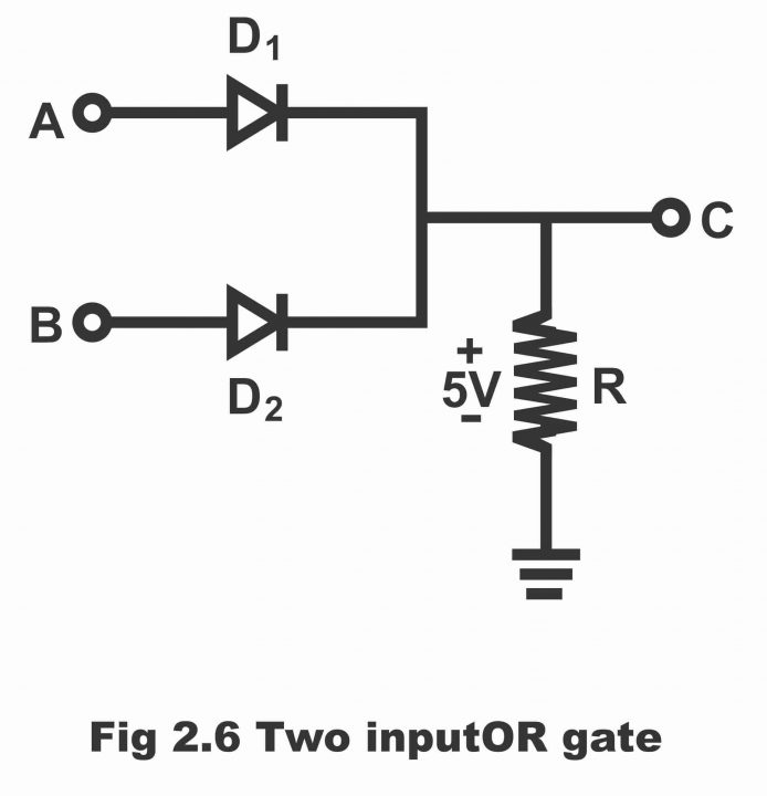
Figure 2.7 Three input OR gate

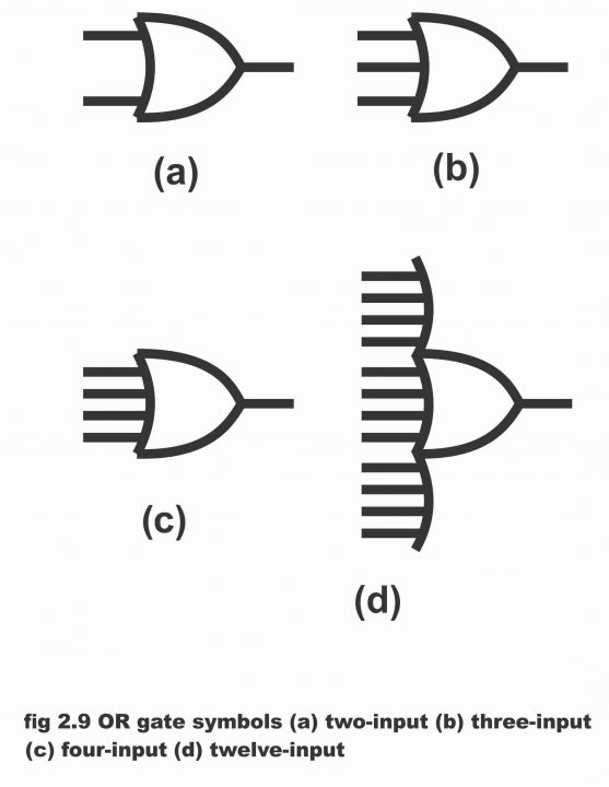
Note: There may be more inputs on an OR gate instead of just two inputs as have been exemplified. For example, if three inputs A, B and C exist on OR gate (as has been depicted in figure 2.7), then in case all three inputs are low, none of the diodes conducts. Thus, output (Y) becomes low. On the contrary, if any one of the three inputs are high, we get high output (because in this situation, diode with a high input only conducts). The possible input and output states of a three-input logic circuit can easily be understood with the help of a truth table as has been given in figure 2.8. In diagram 2.9, various symbols of a OR gate comprising different inputs have been displayed.
Truth Table of Three Input OR Gate
| A | B | C | D |
| Low | Low | Low | Low |
| Low | Low | High | High |
| Low | High | Low | High |
| Low | High | High | High |
| High | Low | Low | High |
| High | Low | High | High |
| High | High | Low | High |
| High | High | High | High |
Table of Binary Equivalent
| A | B | C | Y |
| 0 | 0 | 0 | 0 |
| 0 | 0 | 1 | 1 |
| 0 | 1 | 0 | 1 |
| 0 | 1 | 1 | 1 |
| 1 | 0 | 0 | 1 |
| 1 | 0 | 1 | 1 |
| 1 | 1 | 0 | 1 |
| 1 | 1 | 1 | 1 |
Figure 2.9- OR gate symbols (a) two-input (b). three input (c). four input (d). twelve input
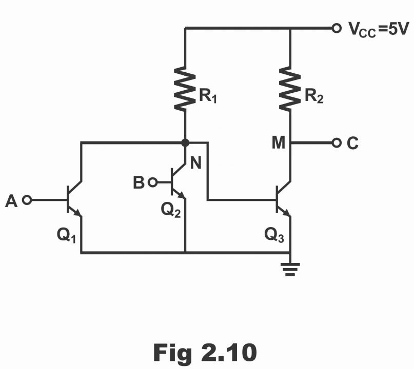
Transistor OR Gate
In figure 2.10, the circuit of a transistor OR gate consisting of three inter – connected transistors Q1, Q2 and Q3, which has been provided a common supply VCC = +5V, has been shown. In this circuit, inputs A and B and output C is vividly visible. The working methodology of this circuit is as follows:
- When +5V are provided on input A, transistor Q1 conducts due to being forward biased. Presume that Q1 has saturated, in such a situation whole of VCC (i.e. 5V) drop parallel to R1. As a result, the voltage value at point N becomes zero (i.e. N point becomes grounded). As N point has been fitted with the base of Q3, thus Q3 cut – off due to a grounded point N. Resultantly, full VCC voltage (i.e. +5V) are received on point C.
- When B is provided +5V, the transistor Q2 conducts and point N goes back to the ground level (i.e. its value becomes 0V). Q3 cuts off due to no forward bias on its base, thus +5V of VCC are received on point C again.
- If both inputs A and B are grounded, both Q1 and Q2 transistors become off and +5V are received on point N. Consequently, Q3 becomes forward biased, and it starts conducting thoroughly. In such a situation, a full VCC drop occurs parallel to R2, due to which point M and C become grounded (i.e. they go to zero volt). Thus, zero volts are received on output C.
Figure 2.10
Previous Topic: Logic AND Gate Working Principle & Circuit Diagram
Next Topic: Logic NOT Gate Working Principle & Circuit Diagram
For electronics and programming-related projects visit my YouTube channel.
Discover more from Electronic Clinic
Subscribe to get the latest posts sent to your email.