Logic NOT Gate Working Principle & Circuit Diagram
Last Updated on September 18, 2022 by Engr. Shahzada Fahad
Table of Contents
The NOT Gate or Inverter
NOT gate is such a digital circuit or gate, which consists of just one input and one output. As this gate inverses the input (that’s its output is not equal to its input) therefore due to the inverting input signals, it is also known as an inverter. In other words, output of a NOT gate is always converse to its input (i.e. if input is 1, output is zero and if input is zero, output will be 1), therefore it is called a NOT gate. It must be remembered that NOT gates’ process of inversion is also called Negation or Complementation, because binary 1 and binary 0 are inverted to each other. In figure 2.18 (a) symbol of a NOT gate or Inverter and figure (b) its truth table has been shown. It is clear from the figure that input and output are mutually reversed or complementary. The symbol of a NOT gate as has been shown in the figure (a) resembles symbol of a triangular or an amplifier. However, a small circle or bubble can also be seen drawn on this triangle, which reveals inversion. It is worth mentioning here that if this small circle or bubble had been drawn in the beginning of the triangular symbol instead of at its end, even then it would have meant inversion.
Figure 2.18 – NOT gate (a) symbol (b) Truth table
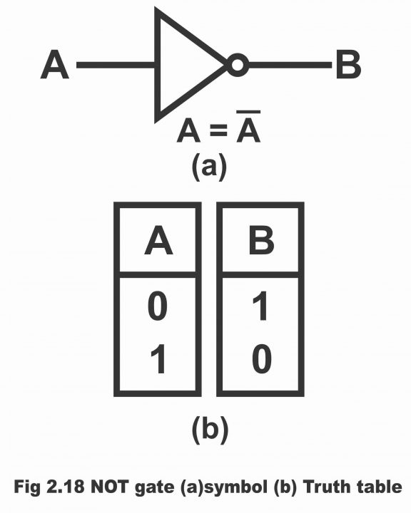
The logical symbol of a NOT gate is denoted via placing a bar above the function, which indicates inverse or opposite state of the input. For example, A means NOT A, similarly, (A+B) imply (A+B) complement or inverse. However, sometime, A is also represented as simply A.
| Output is always the complement of the input |
Or
| When the input is low, the output is high and vice versa |
Boolean Expression
We know that a variable can either be zero or 1 in Boolean algebra, which in terms of digital circuits means that a signal can either be low or high. On the basis of Boolean algebra, the Boolean equation/expression of NOT gate can be represented as under.
| B = NOT A |
If A is zero, then … B = NOT 0 = 1
On the contrary, if the value of A is 1, then … B = NOT 1 = 0
As the bar placed above an output in the Boolean algebra represents NOT operation, therefore above – mentioned equation can also be written as:
| B = A |
i.e. B equals to the complement of A
Transistor NOT Gate
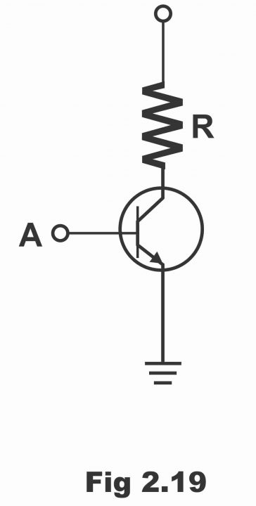
In figure 2.19, a transistor NOT gate circuit has been shown, which consists of a common emitter bipolar junction transistor (BJT). Transistor NOT gate has an input A and an output B. The working methodology of this gate is as under:
When +5V are provided on input A, it fully turns ON (i.e. it starts conducting) due to the reason that EB junction of transistor is forward biased. Thus, maximum collector current is received (i.e. maximum or extreme current passes through the collector). As such, all voltages (i.e. VCC = 5V), due to the flow of maximum current through R on the circuit,
drop parallel to R. As a result, an inverted output is received or output B comes to be on zero level or it becomes ground (i.e. exactly inverted 0 volts are received on output as compared to the input)
When zero volts are provided on input A (i.e. when input A is grounded or on zero level), the transistor does not conduct or it becomes off (because of providing 0 volts on its input, its EB junction does not forward bias) and +5V are received on output B (that’s output is at level 1). Thus, an inverted output is received relative to inputs in any situations.
Figure 2.19
Previous Topic: Logic OR Gate Working Principle & Circuit Diagram
Next Topic: Logic NOR Gate Working Principle & Circuit Diagram
For electronics and programming-related projects visit my YouTube channel.
Discover more from Electronic Clinic
Subscribe to get the latest posts sent to your email.

Output B is missing in Fig.2.19