Logic NOR Gate Working Principle & Circuit Diagram
Last Updated on September 18, 2022 by Engr. Shahzada Fahad
Table of Contents
The NOR Gate
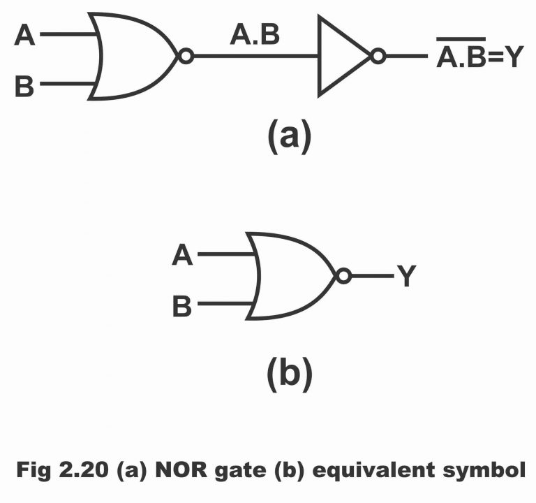
If an inverter is fixed on the output side of an OR gate, it becomes a NOR gate. In other words, NOR gate is actually a NOT-OR gate which is made by fixing an inverter on the output of the OR gate. In figure 2.20, its logic symbol and truth tables has been shown. In the logic symbol of a NOR gate, a small circle or bubble has been made at the end of OR gate, which reflects the process of inversion. From the truth table of NOR gate, it is clear that when any of the input is at 1, the output is zero. Remember that this operation of NOR gate is exactly opposite to the operation of an OR gate, because in case of OR gate, when any input is 1, the receiving output will also always be 1 (that’s NOR function is absolutely inverted to OR function)
Figure 2.20 – (a). NOR gate (b). equivalent symbol (c). truth table
It is necessary to remember that NOR gate is such a useful logic element that it can also be used as a universal gate. That’s AND, OR and Inverter operations can also be carried out with the help of a NOR gate.
Logic Expression
The output equation or Boolean expression of NOR gate can be represented as follows:
| C = A+B or A+B = C |
i.e. C equals to NOT A OR B or C equals to the complement of A OR B
The afore – mentioned expression reveals that first of all two input variables A and B, perform the function of OR gate, and afterwards they become complemented or inverted, as can be seen through a bar above OR expression. Remember that bar above A+B reflects inversion or complement of inputs A and B. As this circuit comprises an OR gate, followed by an inverter, therefore there is just one method of getting a high output from it, that both of its inputs should be low. If any of its input is high, output will be low.
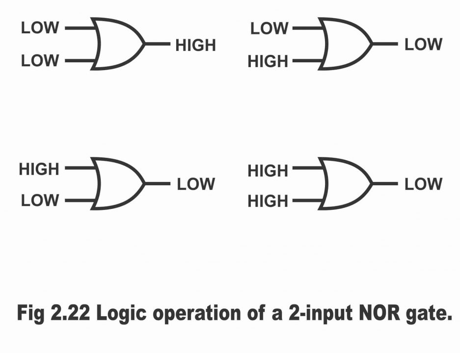
Logic Operation of the NOR Gate
- When any input of the NOR gate is high, the gate produces low output
- When all inputs are low, output is high
- When all inputs are high, NOR gate produces low output
It is to remember that the logic operation of a NOR gate is utterly inverted to the operation of an OR gate.
| Any input is one (High), output is zero (Low) |
Figure 2.22 – logical operation of a 2-input NOR gate
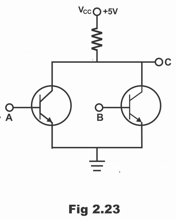
Transistor NOR Gate
In figure 2.23, a transistor circuit identical/ equivalent to a NOR gate has been demonstrated, which consists of two inputs A and B while one output. The working mechanism of a NOR transistor gate circuit is as follows
When both the transistors are cut – off (i.e. when the value of both A and B is zero), output C is 1 at that time. In other words, when both inputs are low simultaneously, a high output (VCC= +5V) is received. However, on the contrary in case of any other input situation (e.g. 01, 10 and 11) either one or both of the transistors saturate, by means of which point C becomes grounded (that’s in case any one or both the inputs are high, output tends to become low or zero as a result of saturation of any one or both of the transistors)
Previous Topic: Logic NOT Gate Working Principle & Circuit Diagram
Next Topic: Logic NAND Gate Working Principle & Circuit Diagram
For electronics and programming-related projects visit my YouTube channel.
Discover more from Electronic Clinic
Subscribe to get the latest posts sent to your email.