Logic NAND Gate Working Principle & Circuit Diagram
Last Updated on September 19, 2022 by Engr. Shahzada Fahad
Table of Contents
The NAND Gate
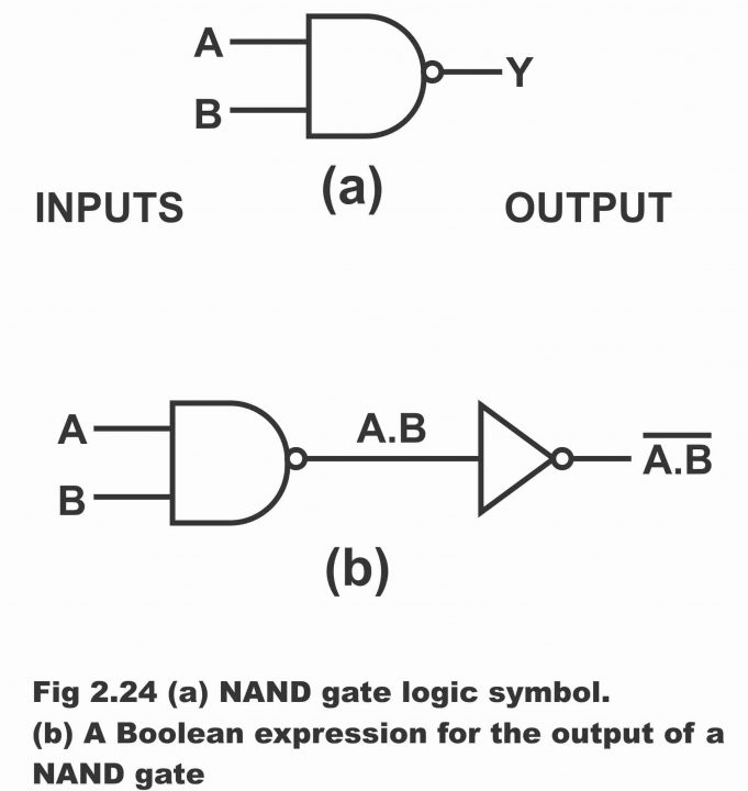
The NAND gate is in fact a NOT – AND gate, which is obtained by mounting a NOT gate on the output of an AND gate. This has been explained with the help of logic symbol as portrayed in figure 2.24 (a) and the Boolean expression in figure (b). In other words, a gate which performs inverted AND function, is called NAND gate. In figure (a), a small circle or bubble made on the NAND gates’ logic symbol’s output, can be seen, which reflects the inversion function of AND gate. Remember, a NAND gate is also used as a universal gate (that’s a required logic junction can be obtained through mounting it on any basic gate), therefore its application in industry is deemed as a phenomenal.
Figure 2.24- (a). NAND gate logic symbol (b). A Boolean expression for the output of a NAND gate (c). Truth table for AND & NAND gate
Truth Table
The truth table of a NAND gate has been shown in the figure ©. In this figure, truth table of AND gate is also visible alongside truth table of the NAND gate, so that a comparison between outputs of the two gates could be drawn. It is obvious from the truth table that all outputs of NAND gate are inverted to the all inputs of a AND gate. In other words, when all inputs of NAND gate are high (or level 1), the output of this gate turns out to be low (or zero) at that time (though, output of AND gate is high, in such a situation 1). However contrary to this, in case any one or both inputs of the NAND gate are low (or zero level), the output to be received from a NAND gate will always be high (or on level 1). If the output column of the NAND gate’s truth table is carefully studied, we come to know that line or row number 4 is only such line, which is at zero level, whereas the output in rest of the lines is 1.
| Any input is zero (low), output is one (high) |
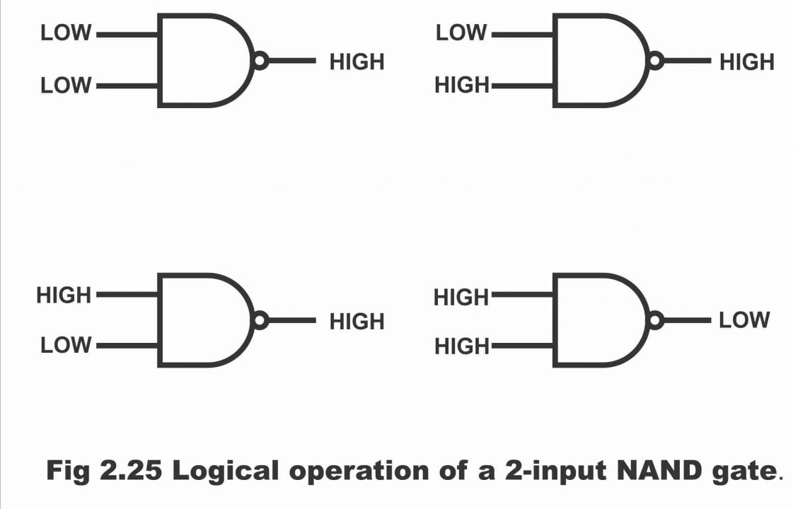
Logic operation
- when all inputs are high, output of the NAND gate is low
- When any one of the NAND gats’ inputs is low, its output is high
- When all inputs are low, even then output of the gate is high
Remember that from perspective of output level, logic operation of NAND gate is totally different from the logic operation of a AND gate. As an active output level in a NAND gate is low level or (zero level), as can be seen via a bubble drawn above the output. The logical operation of a two inputs NAND gate has been displayed in the figure 2.25.
Figure 2.25 – logical operation of a 2-input NAND gate
Boolean Expression
The Boolean or logic expression of two – inputs NAND gate is illustrated as under:
| C = AB or AB = C |
The afore–mentioned expression obviously tells us that two input variables A and B first perform the function of AND, then they get inverted or complement, as is visible from a bar placed above AND expression.
NAND Gate Using Diode – Transistor logic
If a NAND gate comprising two input diodes and a transistor invertor or transistor NOT are inter-connected to form a circuit, this circuit is called a DTL NAND gate. This has been shown in the figure 2.27. the working mechanism of this circuit is as under:
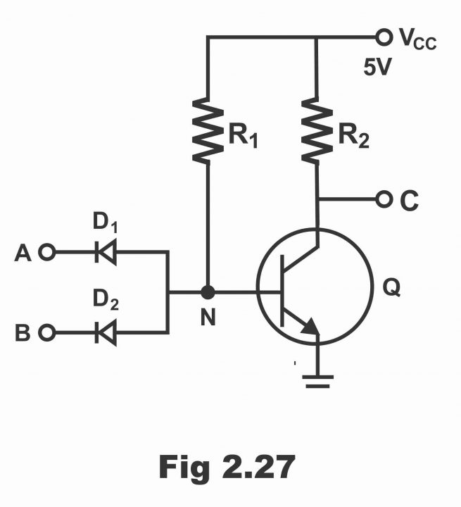
When diode D1 or diode D2 or both diodes conduct, then point N becomes ground. That’s potential of point N becomes zero (the input states have been shown as 10, 01 and 11 in the truth table). Under such a situation, transistor Q becomes off and supply voltage (VCC = +5V) are received on output C (that’s output becomes high or level 1).
When the value of input voltages being provided on A and B is +5V (i.e. when A =1 and B =1), then +5V are received on point N. These voltage on N point are also found on the transistor’s base. Thus, transistor gets saturated when +5V are received on the transistor’s base and zero volts are obtained on output C (that’s to say the output becomes low or reaches the zero level, due to saturation of the transistor)
Previous Topic: Logic NOR Gate Working Principle & Circuit Diagram
Next Topic: Exclusive OR gate (XOR) Working Principle & Circuit Diagram
For electronics and programming-related projects visit my YouTube channel.
Discover more from Electronic Clinic
Subscribe to get the latest posts sent to your email.

