Multiplexer or Data Selector with circuit diagram and operation
Last Updated on November 11, 2022 by Engr. Shahzada Fahad
Table of Contents
Multiplexer or Data Selector
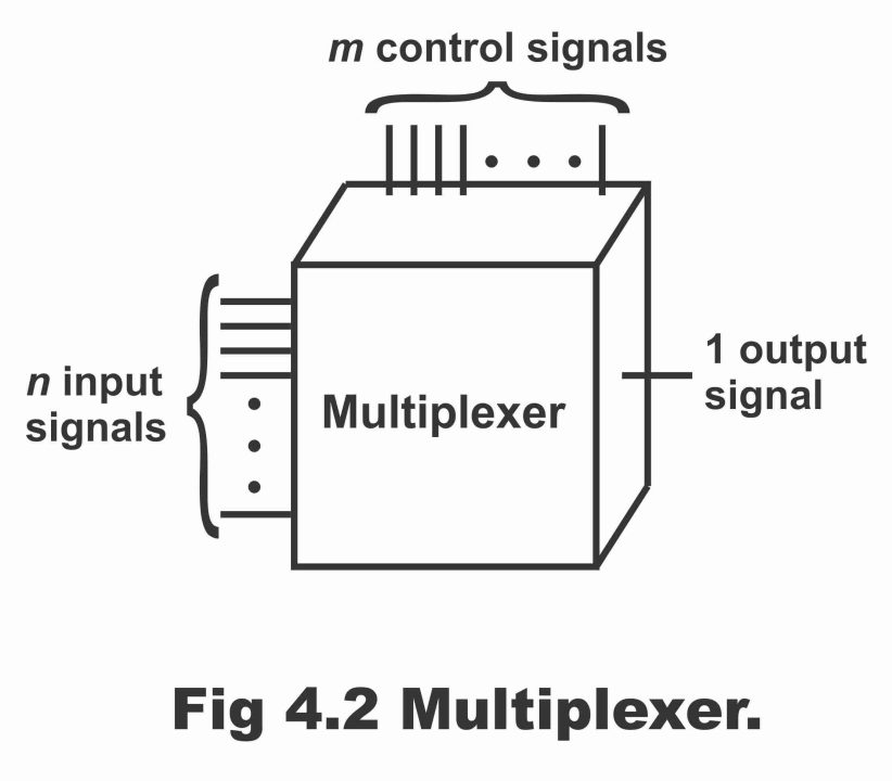
A multiplexer is a logic circuit or device, which selects one input line out of numerous input lines and lets it pass through the output line. Or it is a combinational logic circuit, which selects binary data or binary information from one input line out of several input lines and pass on this data to a single output line, is called multiplexer or Data Selector. In simple words, an electronic circuit, which selects just one input from a number of inputs at a time, and then provides it on output, is known as multiplexer. Any input can transmit on output by means of using control signals. Multiplexers can also shortly be expressed as MUX. As it is a digital circuit, which chose just one channel input from among numerous channel inputs, therefore it is called a data selector. Remember that multiplex means “many into one” and multiplexing means transmitting a very large number of information units through smaller channels or very few lines. The selection of a signal or a specific input line is controlled via control signals or a set of selection lines. Normally, “n” is input signals or input lines and “m” are control signals or selection lines, through the bit combination of which, it is decided which of the input has been selected. This has been manifested in figure 4.2. This particular circuit comprises “n” input signals, “m” control signals and 1 output signal.
Figure 4.2 – multiplexer or Data Selector
The simplest form of a multiplexer resembles a one pole mechanical rotary switch (e.g. ceiling fan’s rotary switch or a TV channel etc.), which has so many or numerous positions, however, you can select just one position of fan or select just one TV channel at a time out of a number of TV channels received, as has been depicted in the figure 4.3
Figure 4.3
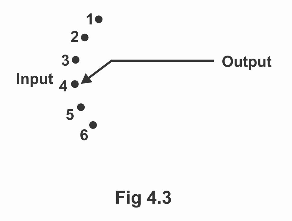
In this figure, a mechanical rotary switch or a rotary selector switch has been shown being used as a multiplexer. Any one of the given six inputs (the number of inputs may be less or higher) can be connected to output by means of adjusting position of the rotary switch (or by rotating it through hands). Thus, input on which the selector switch is connected, only that particular input, output is received. As such a multiplexer or Data Selector can also be defined as “many into one’. As the speed of such type of mechanical rotary switch or mechanical multiplexer is very low and these are also not automatic, thus for performing a faster and an automatic multiplexing operation, digital multiplexers are fabricated with the help of logic gates.
Numerous digital multiplexers ICs are as under:
74150 16 to 1 multiplexer/data selector
74151 8 to 1 multiplexer (with inverted output)
74152 8 to 1 multiplexer/ data selector
74153 Dual 4-line to 1-line multiplexer
74157 Quad 2- line to 1 – line multiplexer
Remember that a multiplexer is generally used to convert a parallel data into serial data
4-to-line multiplexer or Data Selector
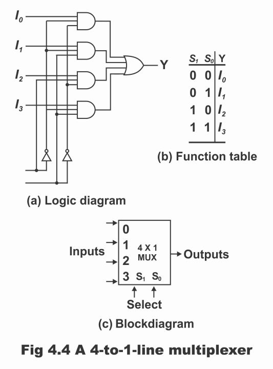
In figure 4.4, the logic diagram, block diagram and function table of a 4 – bit multiplexer or data selector have been shown. In this circuit, every input line out of the four input lines (I0 to I3) has been connected with an input of AND gate. Selection lines are S1 and S2, which have been decoded in such a way that they can select a specific AND gate during a given time or they can control or select a specific AND gate. The function table shown in the figure (b) indicates input and output path for every possible bit combination of the selection line (in other words function table specifies the path, by means of which the signal of the selected input reaches output). When this MSI function is applied in the designing of a digital system, it is represented in the form of a block diagram as has been shown in figure (c).
Figure 4.4 – 4- to -1 multiplexer a. logic diagram b. function table c. block diagram
Operation
- when binary state 0 occurs on data select lines (i.e. S0 = 0 and S1 = 0), two out of the three AND gate inputs connected with I0 via inverter, become 1. However, 3rd input becomes 0 on output because of binary 0 on I0 (as AND gate is a series gate, its output becomes 1 when all of its inputs are 1. In case any one of its inputs is 0, output also becomes 0). As such data present on input I0, reflects on the output line or in such a situation, output of OR gate equals to I0 (i.e. 0) (remember that OR gate is a parallel gate. if any one of its input becomes 1, its output also becomes 1)
- When binary 1 state occurs on data select lines (i.e. S0 = 1 and S1 = 0), in such a situation, AND gate’s three inputs connected to I1 become 1, as a result output of this AND gate become 1. As output of AND gate is the input of an OR gate, therefore in case output of AND gate becomes 1, output of OR gate also become 1. Therefore, data present on I1 input, is received on output line. Remember that during this process, apart from an AND gate connected to I1, at least one of the inputs of other three AND gates is equal to 0, due to which their output also remains 0.
- When there is a situation of S1S0 = 10, or when a binary 2 state occurs on the data select lines i.e. S1 = 1 and S0 = 0, then two out of the three inputs of I2 AND gate become 1, whereas 3rd input remains connected to I2. Under such a situation, At least one of the remaining three AND gates’ inputs equals to zero, as a result their output also becomes zero. Thus, output of OR gate now equals the value of I2 (i.e. 1), thus such a selected input (i.e. I2) gets a passage, by means of which it reaches output. As multiplexers selects one input out of several inputs, and provides a path to transmit its binary information to output line, therefore it is called a data selector. Remember that outputs of a AND gate is received by a single OR gate, which supplies a single output or line – 1 output. (figure a)
- When binary 3 is provided on the select lines (i.e. S0 = 1 and S1 = 1), in such a situation all three inputs of AND gate connected to I3, become 1, whereas at least one of the three AND gates input, becomes 0. As such, output of I3 AND gate becomes 1 while the outputs of remaining three AND gates become zero. Resultantly, data output line present on I3 input, connects. A complete detail about operation of this kind of a circuit, has been illustrated via a function table or truth table in figure (b).
8-to-1 line multiplexer or Data Selector
In figure 4.5, logic diagram and logic symbol of an 8 – inputs multiplexer has been illustrated. It is clear from this figure that this circuit has 8 data input lines and three data select or control lines, whereas it has one output line, along which another inverted output line has also been shown. As we need active low output for some of the applications and active high output for certain others, therefore this kind of facility has also been inducted on this particular circuit. Remember that AND gates and inverters in multiplexers resemble in appearance to a decoder circuit and in fact, they decode input selection lines. Similar to a decoder, there is an enabled input in multiplexer ICs, which control functioning of the unit. When enabled input is in a given binary state (i.e. 1), circuit does not operate at all (i.e. output is disabled in such a situation). And when enabled input is in its other state (i.e. 0) or in its enabled – state, the circuit operates as a normal multiplexer. Enable – inputs are also occasionally known as “strobe”. In figure (a), outputs of all AND gates are received by a NOR gate, which has an output 1 at that time, whereas all of its inputs are zero or its output is 0 at that time, when any one of its inputs or two or three inputs are 1.
Operation
According to the figure, entire data inputs D0 to D7, have been loaded in parallel and out of 8 data inputs, any one is selected in order to provide three binary bits (ABC) on output. In case enabled inputs are high, all gates 1-8 stops working and when it is low, all gates start operating. Three-bit binary input word (ABC) lets only one gate out of the eight to operate according to the input code and provides input on output of that gate only. In such a condition, output of remnant 7 gates is zero. This binary word comprising three input tends to code an address, which decides which of one of the data input lines from D0 to D7 will be selected or operated. (In other words, for selecting any one input signal out of 8 – input signals, we need a 3 – bit address). Six inverters on data select input lines, produce normal and complement signals, which require gates (1 – 8). In the figure, data output and its complement both have been given.
Figure 4.5 – the 74151A B input data selector/ multiplexer
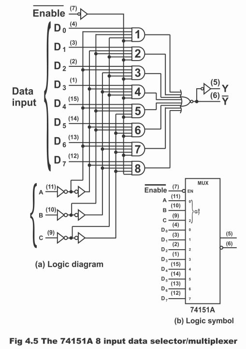
When a state of binary 101 happens on the control lines or data select lines (ABC), then data input line D5 is selected (because 1×22 + 0x21 + 1×20 =5). Thus, the entire data existing on input line D5, is received on the output line in normal and complement form.
When a condition of binary 011 creates on data select lines, then data input line D3 is selected (because 0x22 + 1×21+ 1×20 = 3). As such, all data present on input line D3 is received on output line. Remember that circuit has been designed in such a manner that data only of the selected line is transferred to output line. Whereas under such a situation, all gates except the one connected with the selected line, remain disabled (or they do not operate)
74150 0r 16-to-1 Multiplexer or Data Selector
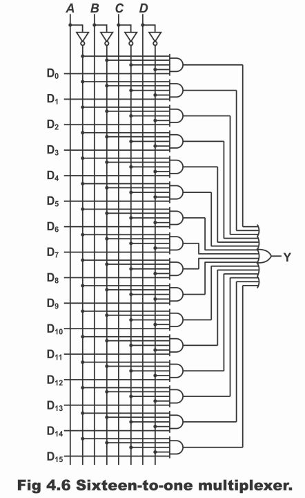
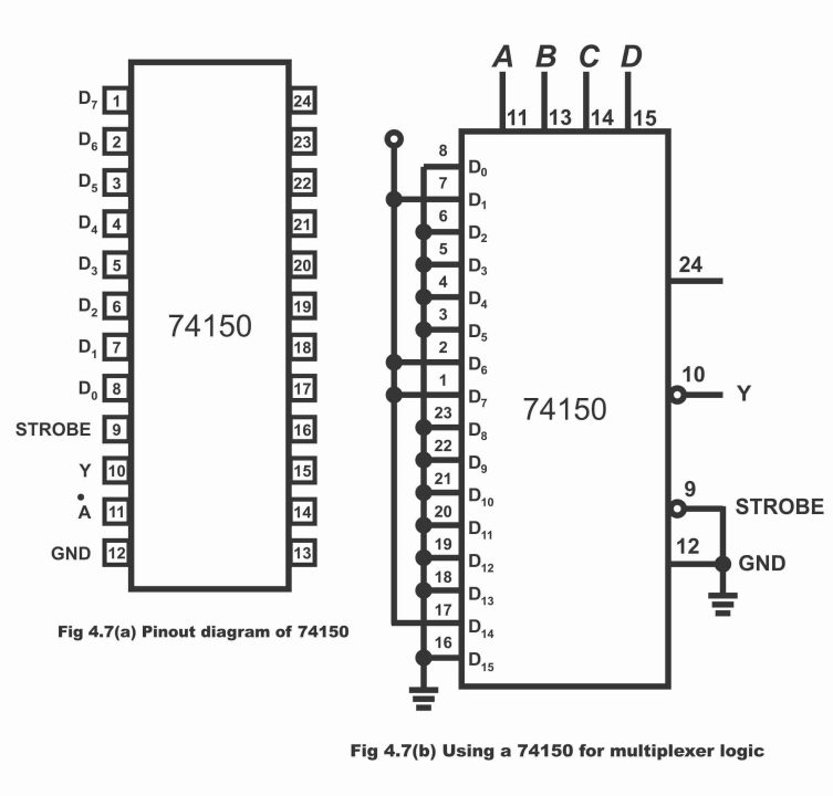
As the name implies, it is a type of multiplexer, which consists of 16 data inputs, four data select lines and only one output (i.e. this multiplexer selects just one input out of 16 inputs at a time and provides it on output line). In terms of ICs, its number is 74150. The logic diagram of a 16 – to -1 multiplexer in figure 4.6, its pin – out diagram in figure 4.7 and truth table in figure 4.8 has been illustrated.
Figure 4.6- 16-to-1 multiplexer
The pin diagram displayed in figure 4.7 (a) is the pin – diagram of the TTL 74150 multiplexer, in which all pins 1 – 8 and 16 -23, are reserved for input data D0 to D15, whereas pin numbers 11, 13, 14, and 15 acts as control bits or selection bits for ABCD. Pin number 10 is specific for output, which provides a complement of the selected bits. Pin number 9 is for strobe, which enables a multiplexer (i.e. lets it work) or disables it (i.e. does not allow it to work or operate). It is evident from the truth table of 74150 given in figure 4.8, that when the strobe is low, the multiplexer operates during that period of time (i.e. when the strobe is low, the multiplexer having been enabled, starts providing output). As a result of the multiplexer operation, an output Y is obtained from it, which is a complement of the input data. On the contrary, when the strobe is high, the multiplexer does not operate (i.e. multiplexer disables during such a situation and does not have any sort of impact on control data ABCD)
Figure 4.7 – (a). pin–out diagram of 74150. Figure 4.7 – (b). using a 74150 for multiplexer logic
Operation
We know that out of the entire input bits (D0 – D15), at a time only that particular one bit transmits towards output, which has been selected by means of control inputs ABCD. For example, if the value of ABCD is 0000 (i.e. ABCD = 0000), in such a situation, the topmost gate is enabled, while rest of the gates get disabled (i.e. only the topmost AND gate, which is connected to D0, operates and rest of the gates do not operate). In other words, when ABCD = 0000, AND gate associated with D0 gets these values of ABCD as 1111 by means of being inverted via an inverter, due to which output of AND gate becomes 1. As such, output of OR gate also becomes 1, resultantly input data present on D0, transmits to output line. Or binary input data present on D0 gets a path for reaching to output (i.e. Y = D0). Remember that in case D0 is low, output Y will also be low and if D0 is high, Y will also be high (i.e. Y depends on the value of D0).
If the value of control nibble changes to ABCD = 1111 (a collection consisting of 4 – bits is called nibble) all gates except the final AND gate, become disabled. In such a situation, data present on D15 only is received on output i.e. D15 = Y
When the value of ABCD is 0111 (i.e. ABCD = 0111), then by carefully looking at the logic diagram, it can be understood that in such a situation AND gate connected with D7 data input, becomes active or enabled, whereas rest of the gates other than D7, become inactive or disabled (because 0x23 + 1×22 + 1×21 + 1×20 = 0 + 4 + 2 +1). Thus, data present on D7, connects on output i.e. Y = D7.
Note: if the 16 – inputs OR gate shown in the logic diagram figure 4.2 is replaced with NOR gate, in such a situation, we get a complement of selected data bit instead of actual data bit on the output, i.e. we get an output utterly in contrast with the above – mentioned explanation. Therefore, if D0 is low, then using NOR gate instead of an OR gate, D0 becomes high. Or the complement of D0 is obtained.
For example, when ABCD = 0111, output is equal to the complement of D7 i.e. Y = D7. It is a Boolean expression of a transistor-transistor logic (TTL) multiplexer, because an inverter is being mounted on the output of such type of circuit, which is complement of the selected data bits.
Previous Topic: Combinational logic & Data Processing circuits
Next Topic: Demultiplexer or Distributor with circuit diagram and operation
For electronics and programming-related projects visit my YouTube channel.
Discover more from Electronic Clinic
Subscribe to get the latest posts sent to your email.

very good and understandable