Integrated Circuit, Analog IC, Digital IC, and Manufacturing of ICs
Last Updated on September 12, 2021 by Engr. Shahzada Fahad
Table of Contents
Integrated circuit, Overview:
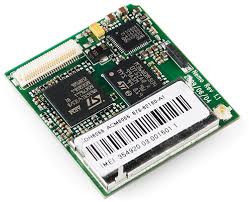
Integrated circuits have a big role to play in miniaturization of electronic gadgets. Earlier the electronic circuit was prepared using transistors, diodes, and resistors by joining those using conducting wires because of this these circuits were huge and bulky. Further these circuits were not reliable so an attempt was to fabricate an entire circuit consisting of many components such as diodes, resistors, inductors, capacitors on a small block of semiconductor connected with the help of metal strips. This give raise the concept of integrated circuit IC. IC’s are found in almost all gadgets like cars, television, CD players and cell phones. The size of an IC is 1mm by 1mm being so small in size. IC’s have made the miniaturization of electronic gadgets possible. When we opened up an electronic device we see many ICs for example microcontroller in DVD player or PWM IC on a power supply. Even if we say that electronics is incomplete without an IC than it is correct because IC is like a backbone in electronics circuit. In order to make integrated circuits we will need thousands of electronic components like resistor, capacitor, diode and transistors. They are directly formed on a sheet of silicon so that they can get shape of IC. Now if discuss about its types they are divided in to two groups which are:
-
Square IC
The example of square IC is atmega328 which has pins on its entire four sides in some IC it contains 80 Pins and in some it contains 100 pins. Even these pins can reach up to 500.
-
Rectangle IC
It has pins on only two sides due to which it is called rectangular IC. If someone asks you that how many transistors, diodes, capacitors, resistors are there in the IC. It will be impossible for you to guess the exact amount.
If we see the structure of the 555 timer there are a total of 23 transistors, 15 resistors and a couple of diodes. We can see how they managed to fix all these 23 transistors and 15 resistors in this small IC. Although if we break this IC and see all these components in the IC. They are formed in form of sheet of silicon in such a way that we cannot see with our naked eye.
Now the question arise in our mind what is the fun of making these ICs if we can make it by using schematic diagram and make the whole circuit by using the same amount of the resistors and transistors then it would take the entire bread board to make the whole circuit. So due to integrated circuit we place large circuit in a very small IC and can use the same circuit in very less space. The integrated circuit does not contain coils and transformer the reason for this is due to their large size making them in very small size is very expensive as compared to other components like resistors, capacitors. So due to which the designer avoid it to use it in ICs and use it externally in the circuit.
History of the Integrated circuits:
From roughly the 1940’s through the mid 1960’s every computer consists of discrete components which were all wired together and in 1958 Jack Kilby first invented integrated circuit. For example the ENIAC consists of more than 17000 vacuum tubes, 70000 resistors, 10000 capacitors and 7000 diodes all of which required 5 million hand soldered collections. Adding more components to increase performance meant more connections, more wires and just more complexity.
By the mid 1950’s transistors were becoming commercial available and being incorporated in to computers. These were more much smaller, faster and more reliable than vacuum tubes but each transistor was still one discrete component.
In the 1959’s IBM upgraded their vacuum tube based 709 computers to transistor by replacing all the discrete vacuum tubes with discrete transistors. The new machine the IBM 7090 was six times faster and half of the cost. These transistorized computers marked the second generation of electronic computing. However although faster and smaller discrete transistor did not solve the tyranny of numbers.
Earlier the size of the computer used to be very big however now day’s laptop computers and palmtop computers are available wondering.
IC’s can be grouped in to two categories depending on the nature of input signals which are:
- Linear or analog IC’s
- Digital IC’s
In linear IC’s the input are analog signals which change smoothly and continuously over range of values between a maximum and minimum. In this case the output is directly proportional to the input which will vary with input. Operational amplifier is an example of linear IC. In digital ICs the input signals are digital signals that have only two values. They contain circuit such as logic gates based on the number of logic gates present in it. Digital IC’s can be further classified as:
- SSI (small scale integration)
- MSI ( medium scale integration )
- LSI ( large scale integration )
- VLSI ( very large scale integration )
VLSI:
Very large scale integration is the process of creating an integrated circuit. when we think about circuit a printed circuit board come in our mind on which various types of components like capacitors, transistors, diodes, resistors etc are soldered this is called discrete circuit in which we have discrete components. In contrast the integrated circuit the entire circuitry that is the active and passive elements by active components we mean transistors. It can be bipolar junction transistor or field effect transistors are housed on the same substrate. VLSI consist of thousands of transistors in a single chip. We have seen the memory card in our phone which is also VLSI. VLSI begins in the 1970s when the complex semiconductor and communication technologies were being developed. The microprocessor is a VLSI device. An electronic circuit might consist of a CPU, ROM, RAM and other glue logics. VLSI lets IC designer add all of these in to a one chip.
Small Scale integrated circuit:
When we consider a circuit which has about 10 to 100 transistors or logic gates per square millimetre in it then it is called small scale integrated circuit.
Medium Scale integrated circuit:
When we have a circuit which has about 100 to 1000 transistors in it then it is called Medium scale integrated circuit.
Large Scale integrated circuit:
When we have a circuit which has more than 10000 transistors in it then it is called large scale integrated circuit.
Very Large Scale integrated circuit:
When we have a circuit which has more than 4 million transistors in it then it is called very large scale integrated circuit.
More than 25% of today VLSI chips are made up of silicon. Silicon is group 4 element of the semiconductor. It has number of very desirable properties. Active element in the integrated circuit is the most important element. When we talk about very high speed circuit we usually have bipolar junction transistors in them. BJTs have very high speed and when we talk about very high packing density we usually we usually talk about MOSFET like DRAM chip which is based on the MOSFET technology. So essentially we can say that VLSI technology can be classified in to branches:
- BJT technology
- MOSFET technology
When the circuit complexity is increasing and our requirement becoming more and more stringent we are moving towards these two technologies, which bring about the newest on the horizon. The BIMOS or BICMOS technology in which the same circuit may have some active elements as bipolar junction transistor and some have field effect transistors. If we need high speed we will use bipolar junction transistor and if we need high density we will use MOSFET.
Manufacturing of IC Integrated circuits:
Now we look at the steps followed in the manufacturing of IC’s.
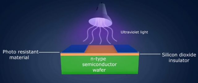
Firstly a wafer of N-type semiconductor is taken and photolithography technique is used. In this technique firstly a layer of silicon dioxide insulator is coated over it then a thin layer of photo resistant material is placed over silicon dioxide. After this masking is done and ultraviolet light is made incident on it. Whenever the light is incident over the photo resistive portion it becomes hard and no chemical reaction can takes place over it.
Next silicon dioxide is removed with the help of etching process. Lastly the required impurities are added the process is repeated to obtain different geometries require to complete a chip circuit design. The internal connection between the components is made by passing aluminium vapour. The chip is enclosed in a protective plastic case. Finally with the help of a thin aluminium leads the connectors are taken out and this is how the standard package IC is manufactured. This type of the IC in which the entire circuit is formed on a single silicon crystal is called monolithic IC. These are the mostly wide used IC large number of monolithic IC is embedded on a ceramic substrate is known as hybrid IC.
Manufacturing of Chips:
All chips start with very simple raw material sand. Sand is primarily made up of silicon dioxide or silica. Silicon is the second most abundant element in the earth crust but is only found as a compound with oxygen. Complex chemical and physical processes are required to ensure that silicon crystals meet the high production standard that apply to chips to convert silica sand to silicon. The sand is combined with carbon and heated to an extremely high temperature to remove the oxygen. A number of other steps are required to create the finish products namely an extremely pure mono crystalline silicon ingot called a ball with only one impurity atom for every ten million silicon atoms. Silicon balls are fabricated in a range of different diameters. The most common sizes are 150 mm, 200 mm and 300 mm. Wafers with a large diameters offer a more space for chips extremely thin chips are then cut from the silicon balls using a special sawing technique. These wafers are the basic building blocks for subsequent chip production. Silicon is semiconductor this means it can conducts electricity and also act as an insulator. The pure mono crystalline silicon is nonconductive at room temperature to allow it to become conductive small quantities of specific atoms are added as impurities to the wafer. These impurity atoms must have a number of outer electrons that is either one more or one less than that of silicon.
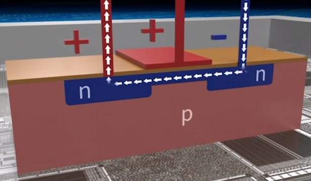
The transistors are built on the P and N conductive layers that exist in a doped wafer. Transistors are smallest control units in microchips their job is to control electric voltage and currents and they are by far the most important component of electronic circuit. Every transistor on chip contains P and N conductive layers made up of silicon crystals. They also have an additional layer of silicon oxide which act as an insulator. A layer of electrically conductive poly silicon is applied on top of this. Every transistor has three terminals the middle one is attached to the gate which is electrically conductive poly silicon. If an electrical charge is applied to the only two outer terminals. Electricity cannot flow as the transistor is blocked this changes however if an additional charge is applied to the middle terminal. Electrons from the P layer are then pulled towards the middle terminal and accumulates at the area bordering the silicon crystal and the insulating gate oxide. A channel then forms underneath the gate between the islands of N conductive material. Electrons can flow through this channel the electrical circuit is closed. In this way the transistor can be switched back and forth between current enable and disable between 0 and 1.
The process to manufacture of chips from the wafers start with layout and design phase highly complex chips are made up of billions of integrated and connected transistor enabling sophisticated circuits such as microcontrollers and crypto chips to build on semiconductor surface measuring just a few square millimetres in size. The sheer number of components for an in depth design process this entails the chip function simulating it technical and physical properties.
Discover more from Electronic Clinic
Subscribe to get the latest posts sent to your email.
