Semiconductor Diodes and its Types
Last Updated on February 5, 2022 by Engr. Shahzada Fahad
Table of Contents
Semiconductor Diodes Introduction
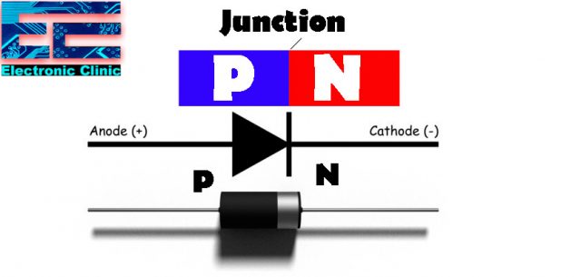
Semiconductor diodes– A diode made of semiconductor components, usually silicon. The cathode, which is negatively charged and has an excess of electrons, is placed adjacent to the anode, which has an inherently positive charge, carrying an excess of holes.
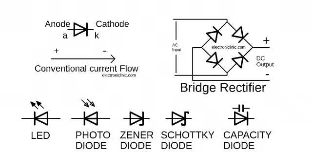
Diode is made up Silicon or Germanium having some impurities that is Pentavalent impurity for N-type and trivalent impurity for the P-type semiconductor. Di means two and Ode means electrodes. Hence Diode is a two electrode device. These two electrodes are called Anode and Cathode. As it is a PN junction, so ‘P” is referred as Anode (having holes or +Ve charges) and N is referred as the Cathode (having electrons or –Ve charges). The diagram for PN junction Diode is given as.
When a Diode is forward biased it offers very low resistance and hence conduction will take place and it will act as a conductor. When a Diode is reversed biased i.e when the Ground is connected with the Anode and Positive of the supply is connected with the cathode, it offers very high resistance and will not conduct. Hence it will act as insulator. So we can say that Diode is a one-way device with two terminal Anode and Cathode as shown in the fig above.
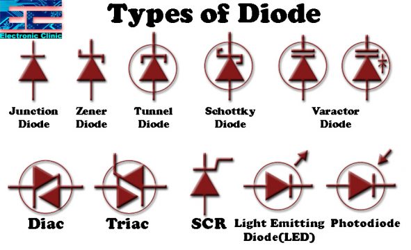
The Arrow head shows the direction of the conventional current when it is forward biased. Every Diode has its own identification and specification. There are different types of diodes.
- Power Diode
- Zener Diode
- Pin Diode
- General Purpose Diode
- Fast Recovery Diode
- Schottky Diode
- Step Recovery Diode
- Photo Diode
- Varactor Diode
- Tunnel Diode
Power Diodes or Rectifier diodes are a vital component in power supplies where they are used to convert AC mains (line) voltage to DC. These are used in Power electronics for as rectifiers. Diodes can also be used to prevent disastrous damage to battery powered equipment when batteries are connected in the wrong polarity. Zener Diodes are also used as the voltage regulators.
Pin Diodes are used as switching diodes for signal frequencies. Pin Diodes are also used as the amplitude modulation.
General Purpose Diodes are used as frequency convertors that is low frequencies to higher frequencies. Fast Recovery Diodes have low recovery time normally less than 5 micro seconds. These are used in convertor circuits that are DC to AC and AC to DC. Schottky Diodes are used for high current and low voltage circuit power supplies. Step Recovery Diodes are used in digital circuits. These are also used as multiplexers. Photo diodes also produce electrical current from light. Varactor Diodes are used to control the voltage for the tuning of Radio and TV receivers. Tunnel Diodes are used in places where very fast switching speed is required. So it is used in high speed computer memories. It is also used in high frequency Oscillators.
Fig. 1 shows a selection of common wire ended diodes as follows:
- Three power rectifiers, (bridge rectifier for use with mains (line) voltages) and two mains voltage rectifier diodes).
- Point contact diode (with glass encapsulation) and Schottky diode.
- A small signal silicon diode.
- Zener diodes with glass or black resin encapsulation.
- Selection of light emitting diodes. Red to counterclockwise: yellow and green indicator LEDs, infra-red photodiode, 5mm warm white LED and 10mm high brightness blue LED.
Diode Circuit Symbols
As explained earlier a Diode is a uni-directional semiconductor device, provided with two terminals. The two terminals of the Diode are anode or positive terminal and cathode or negative terminal. Ideally a diode will pass current when properly biased i.e. when its anode or positive terminal is more positive than its cathode or negative terminal, while its anode will block current flow when it is more negative than its cathode. In the circuit symbols shown in Fig. 2, the cathode is shown as a bar and the anode as a triangle. In some circuit diagrams the anode of the diode can also be represented by the letter ‘a’ and the cathode by the letter ‘k’.
Which way does diode current flow?
The direction of the current flow can be seen in the Fig.2 that is the conventional current flows from the Anode (positive) terminal to the Cathode (Negative) Terminal, while the motion of the electrons is in the opposite direction, from the Cathode to the Anode of the Diode.
Silicon Diode Construction
A Diode is a Silicon Semi-conductor device and is made up of two different types of materials N-type and P-Type. The N-type semi-conductor is obtained when Penta-valent impurity is added to pure Ge crystal. Each Penta-valent atom forms four covalent bonds with the four electrons of Si or Ge. Out of 5 electrons of penta-valent atom four are combined with the four electrons of Ge or Silicon, the fifth electron is super-fluous (Extra), and is loosely bound with the nucleous of penta-valent atom. So, this electron is also called as free electron. It can be easily excited from the valence band to the conduction band by the application of external energy, that may be electrical energy or thermal energy.
The P-type semi-conductor is obtained when tri-valent impurity (Ga, B) are added to a pure Ge Crystal. The three valence electrons of ‘B’ form three co-valent bonds with the four surrounding Ge. But the fourth bond remains incomplete, which will rise a hole and that will be the vacancy for an electron. So it will accept an electron from the nearby atom. B is called acceptor impurity repeating the process again and again there will be many and many holes. Note that in acceptor letter ‘P’ is for P-type Extrinsic semi-conductor and also ‘P’ for +Ve charge carriers. While in DONOR the letter ‘N’ is for N-type semi-conductor or –Ve charges.
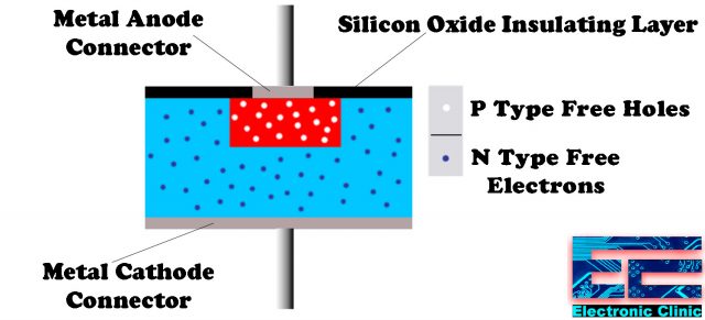
Modern silicon diodes are usually manufactured using one of the different versions of the planar process, which is also used to make transistors and integrated circuits. The layered structure used in silicone planar methods offers many advantages such as predictable performance, reversible performance and reliability and being advantageous for bulk production. The simplified planar silicon diode is described in Fig. 3. Using this process for silicon diodes produces two separate doped layers of silicon, which form a ‘PN junction’. Un-doped or ‘internal’ silicon molecules have a lattice structure that contains four valence electrons, while P-type silicon and n-type silicon are doped by adding a very small amount of material that has a molecular structure with three valence electrons (e.g. boron or aluminum). ) Five valence electrons (e.g. arsenic or phosphorus) to form P type, or N type silicon. These doped versions of silicone are called ‘extrinsic’ silicone. P type silicon now has a valence rat shortage valence electrons in its structure, which can be considered as ‘holes’ or a surplus of positive charge carriers, while N type membrane molecules have five electrons in its valence shell and therefore have a surplus of electrons, which are negative charge carriers.
Diode PN Junction
When a P-type semiconductor material is joined to the N-type semiconductor material the contact surface of the both semiconductors is called PN-junction as shown in the figure below.

The PN junction is obtained by one of the following type of fabrication.
- Crown Junction
- Alloy Junction
- Diffused Junction
- Epitaxial growth Junction
- Point Contact Junction
- Surface Barrier Junction
- Re-crystallized Junction
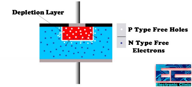
When a PN-junction is packed as a semiconductor device then that will be called PN-junction Diode or Semi-conductor Diode. As Holes are in majority carrier in P-region and Electrons are in majority carrier in N-region.

White represents the Holes and Blue represents the Electrons. When a PN-Junction is just formed some of the holes of P-type will move towards the N-type (where electrons are there) the holes are diffused in electrons and undergo hole-electron recombination. Similarly some electrons of N-type diffuse in some holes of P-type semi-conductor and undergo electron hole recombination. This whole process is called diffusion.
Thus along the junction between P and N type silicon, a small natural potential is formed between the P and N semiconductor materials, with the now negatively charged electrons on the P type side of the junction, and the positively charged holes at the N side junction. This layer of anti-polarity charge carriers is built up to fit more holes or to prevent the free movement of electrons.
This diffusion of holes and electrons across the junction occurs for a very short time. After a few recombinations of holes and electrons at the junction a narrow region called barrier is set up at the inner ends of the P-type and N-type semi-conductors. This barrier will stop further movement of charges. The barrier consists of immobile fixed +Ve and –Ve ions. Hence the region which consists of +Ve and –Ve charges is called the depletion layer or depletion region or resistance, or space charge region.

The size of the depletion region depends on the doping level P-type and N-type semi-conductors. Depletion layer is wide for Heavily doped semiconductor and is narrow for lightly doped semi-conductor. Approximately, it has width of 10-6 m, because of charge separation, that is +Ve charges and –Ve charges, an electric potential called barrier voltage is developed across the junction even if no external source is connected. The barrier voltage is denoted by VB and its value is .3V for Germanium and .7V for Silicon at room temperature.
Therefore when a diode is connected into a circuit the current does not flow between the anode and the cathode until the anode is more positive than the cathode by at least enough forward potential or voltage (VF) to overcome the natural reverse potential of the junction. This value depends mainly on the materials from which the P and N layers of the diode are made and the amount of doping used. Different types of diode have natural reverse potentials ranging from approximately 0.1V to 2 or 3V. Silicon PN junction diodes have a junction capacitance of 0.6V to 0.7V. Begins as shown in Fig. 5.
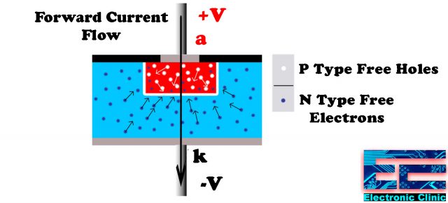
As the applied voltage between the anode and cathode increases, the forward current first slowly increases as the charge carriers begin to cross the attenuation layer and then increase rapidly in an approximately exponential manner. The resistance of the diode is not zero ohms, but very low when operated in ‘On’ or ‘Forward Biased’ mode. Since forward conduction increases after the decrease potential is approximately exceeded in the following exponential curve, the forward resistance (V / I) changes slightly depending on the applied voltage. Reverse Biased Diode When the diode is reverse biased (the anode is connected to the negative voltage and the cathode is connected to the positive voltage), the positive holes are on the negative side of the anode and away from the junction, as shown in Fig. 6.
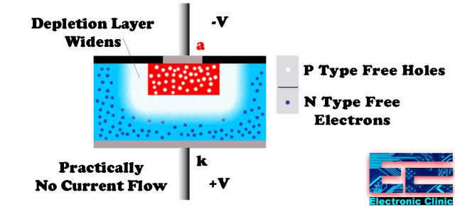
Similarly negative electrons are attracted away from the junction towards the positive voltage applied to the cathode. This action leaves more area at the junction without any charge carriers (positive holes or negative electrons) as the attenuation layer expands. As the junction area is now depleted from the charge carriers it acts as an insulator and as high voltages are applied at the reverse polarity, the attenuation layer changes widely as more charge carriers from the junction. The diode does not apply to reverse voltage (reverse bias), except for very small ‘reverse leakage current’ (IR), which is typically less than 25nA in silicon diodes. However, if the applied voltage reaches a value of ‘reverse breakdown voltage’ (VRRM) current in the reverse direction, the diode will be destroyed if the current is not somehow limited. Diode I / V characteristics the operation of diodes can also be described by a special graph called a ‘character curve’ as described above. These graphs show the relationship between the actual currents and voltages associated with the different terminals of the device. Understanding these graphs will help you to understand how the device works. For diodes, the characteristic curve is called the I / V characteristic because it shows the relationship between the applied voltage between the anode and the cathode and the resulting current flowing through the diode. A common I / V characteristic is shown in Fig. 7
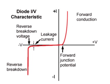
The axes of the graph show positive and negative values and intersect. The intersection has zero value for both current (Y axis) and voltage (X axis). The + I and + V (upper right area of the graph) axes after the initial zero current region show that the current is increasing. This is the forward conduction of the diode when the anode is positive and the cathode is negative. There are no currents at the start until the applied voltage exceeds the forward junction capacity. After this, the current rises well in an approximately exponential manner. The -V and -I axes show the reverse biased condition (lower left area of the graph). It can be seen here that a very small leakage current increases with the increase of the reverse voltage. However, once the reverse breakdown voltage is reached, the reverse current flow (-I) increases sharply.
Diode application
The simplest semiconductor component, the diode, has an astonishing number of applications, starting with many practical and unique diodes that are crucial in modern electronics. Although only two-pin semiconductor devices, there are many applications of key diodes in modern electronics. Diodes are known only for moving current in one direction. This allows the diode to function as a one-way valve, placing the signals where needed or rotating them around the components. While diodes allow only one direction of current, each type of diode works differently, making many useful applications for diodes. Some common applications of diodes are:
- Correcting voltage such as converting AC to AC DC voltages
- Separating signals from supply
- Voltage reference
- A Controlling the signal size
- Mixing signals
- Detection signals
- Lighting
- Lasers diodes
Methodology
An experimental method has been used to research how thermal (temperature) affects the reliability, stability and performance characteristics of this electronic component, even as a circuit, electrical / electronic equipment or as a personal device. In this research I have made it clear that the scope of this research is limited to just one electronic component, which is the diode. This part is subjected to a temperature higher than room temperature (35-65 Celsius) by using a furnace and then connecting wires, breadboards and a Multimeter. The output readings of the temperature rise were then taken with a Multimeter.
Different types of diodes
Let us now briefly look at some of the commonly used types of diodes.
-
Small signal diode
It is a small device with unequal characteristics and its applications are mainly involved in high frequency and very low current devices such as radios and televisions. Also known as glass passivized diode, it is widely used as 1N4148 as it is covered with a glass to protect the diode from contamination.
The appearance of the signal diode is very small compared to the power diode. An edge marked black or red to indicate the cathode terminal. The performance of a small signal diode is very effective for applications at high frequencies.
With respect to the functional frequency coefficients of the signal diode, the carrying capacity of current and power is very low, ranging from a maximum of 150mA and 500mW.
The signal diode is a silicon doped semiconductor diode or a germanium doped diode, but the properties of the diode vary depending on the doping material. The properties of the silicon doped diode in the signal diode are the same as those of the germanium doped diode.
The silicon signal diode has a high voltage drop of 0.6 to 0.7 volts at the junction, so it has a very high resistance but a low forward resistance. On the other hand, the germanium signal diode has a low voltage drop of 0.2 to 0.3 volts and a low resistance due to the high forward resistance. The functional point does not interfere with the small signal diode due to the small signal.
-
Large signal diode
These diodes have a large PN junction layer. Hence the transition of AC voltages to DC is unlimited. It also increases the forward capacity and reverse blocking voltage. These large signals also interfere with the functional point. For this reason it is not suitable for high frequency applications.
The main applications of these diodes are in battery charging devices such as inverters. The forward resistance range of these diodes is in ohms and the reverse blocking resistance is in mega ohms. They can be used in electrical equipment as they have high current and voltage performance, which is used to suppress high peak voltages.
-
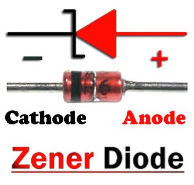
Zener diode
It is a passive element that operates under the genre breakdown principle. First produced by Clarence Jenner in 1934. It is similar to a normal diode in the forward direction, it allows current in the reverse direction when the applied voltage reaches the breakdown voltage. It is designed to prevent other semiconductor devices from transient voltage pulses. It acts as a voltage regulator.
-
Light Emitting Diode (LED)
These diodes convert electrical energy into light energy. The first production began in 1968. It undergoes an electroluminescence process in which holes and electrons recombine to produce energy in the form of light in a forward bias state.
Previously they were used in inductor lamps, but now in more recent applications they are used in environmental and work management. Most commonly used in applications such as aviation lighting, traffic signals, camera flashes.

-
Constant current diodes
Also known as current-regulating diode or constant current diode or current-limiting diode or diode-connected transistor. The function of a diode is to control the voltage at a certain current.
It acts as a two terminal current limiter. This serves as the current limit to achieve high output impedance in the JFET. The constant current diode symbol is shown below.

-
Schottky diode
In this type of diode the junction is formed by the contact of the semiconductor material with the metal. Due to this the forward voltage drop decreases per minute. The semiconductor material is N-type silicon, which acts as an anode and acts as a metal cathode, its materials being chromium, platinum, tungsten, etc.
Due to the metal junction these diodes have a high current carrying capacity, thus reducing the switching time. So, Schottky has more use in changing apps. The voltage drop due to the metal-semiconductor junction is low, which increases the diode performance and reduces the power loss. Therefore, they are used in high frequency rectifier applications. The symbol of the Schottky diode is as shown below.

-
Laser diode
Similar to the LED that forms the active area through the P-N junction. The electric laser diode is a p-i-n diode in which the active region is in the inner region. Used in fiber optic communications, barcode readers, laser pointers, CD / DVD / Blu-ray reading and recording, laser printing.
Laser diode types:
- Double Hetero Structure Laser: Free electrons and holes are available simultaneously in this region.
- Quantum well lasers: Lasers with more than one quantum well are called multi quantum well lasers.
- Quantum Cascade Lasers: These are hetero junction lasers that initiate laser action at relatively long wavelengths.
- Special constrained hetero structure lasers: We go for special constrained hetero structure lasers to replace the thin layer problem in quantum lasers.
- Distributed Bragg Reflector Lasers: This can be edge emitting lasers or viscera.

-
Photodiodes
Photodiodes use junctions between p- and n-type semiconductors. An n-type semiconductor has a lot more mobile electrons, while a p-type material has less mobile, positive holes. When two such materials join, the electrons and holes are pulled to opposite sides of the junction and the energy level structure in the lower fig can be obtained. The area near the junction has virtually no electrons or holes and is called the decay layer.

When the junction is illuminated, the valence-band electrons are excited to the conduction band, creating electron-hole pairs. Due to the strong potential gradient in the junction area, the electrons and holes accelerate in opposite directions and the current flows.
The speed of response and sensitivity of the photodiode can be increased by reverse biasing; the positive side of the battery is connected to the n-type material and the negative side to the p-type material. High sensitivity can be obtained by inserting a layer of high-resistance (internal) material between the p- and n-layers; such a device is called a P-I-N (or pin) diode. Pin diodes have a useful response up to a frequency of a few hundred MHz
With a sufficiently high reverse bias, electron multiplication can occur due to secondary emissions. This effect is used to obtain sensitivity by a few hundred factor in avalanche photodiodes, but at the expense of noise increase at lower light levels. Photodiodes are also available in a package that includes a high-performance operational amplifier. These devices can be used at very low light levels and, unlike photomultipliers, require only low voltage. A linear relationship between the output voltage (and current) and the light level can be obtained over several decades.
Silicon photodiodes are commonly used and have a maximum sensitivity of around 0.8–0.9 around, as shown in Fig. 7.3. Germanium and InGaAs photodiodes are useful in this region from 1.1 to 1.7 m.

Principle of operation
Silicon is a semiconductor with a band gap strength of 1.12 eV at room temperature. This is the gap between the valence band and the transmission band. At absolute zero temperature the valence band is completely filled and the conduction band is empty. As the temperature increases, the electrons become excited and increase by thermal energy from the valence band to the conduction band. Electrons can be amplified to the transmission band by particles or photons with a power greater than 1.12eV, corresponding to wavelengths less than 1100 nm. The electrons in the conduction band are free to conduct current.
Due to the concentration gradient, the diffusion of electrons from the Ntype region to the P-type region and the expansion of the pores from the Ptype region to the N-type region develop a built-in voltage across the junction. The mutual diffusion of electrons and holes between regions N and P across the junction leads to an area free of carriers. This is the area of decline. The built-in voltage in the attenuation area results in a maximum electric field at the junction and no field outside the attenuation area. Any applied reverse bias adds to the built-in voltage and leads to a wide attenuation area. The electron-hole pairs generated by the light are washed away by drift in the decay region and collected by diffusion from the imperfect region. The current output event is proportional to the light or radiation energy. Light is absorbed sharply by distance and is proportional to the absorption coefficient. The absorption coefficient is very high for short wavelengths in the UV region and small for high wavelengths (Figure 2). Therefore, small wavelength photons such as UV combine in a thin upper surface layer, while silicon becomes transparent to light wavelengths greater than 1200 nm. Also, photons with a smaller energy than the

band gap are not perceived all.
Figure 14. Depth of light penetration into the silicon surface for different wavelengths (1 / e).
Applications of diode: –
- Rectifiers
- Clipper circuits
- Clamping circuits
- Current reverse current protection circuits
- In Log Logic Gates
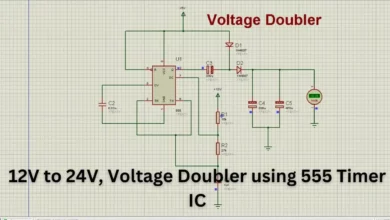
- Voltage multipliers
Discover more from Electronic Clinic
Subscribe to get the latest posts sent to your email.