Adder, Half Adder and Full Adder in Digital Electronics
Last Updated on July 7, 2020 by Engr. Shahzada Fahad
Adder in Digital Electronics, Description:
Adder In Digital Electronics- A combinational circuit that performs the addition of bits is called an Adder. Each computer has an adder located in its CPU(ALU) that is responsible for the process of addition. There are two types of Adder. They are also used in other parts of the processor, where they are used to calculate addresses, table indices, increment and decrement operators, and similar operations.
- Half Adder
- Full Adder
Half Adder:
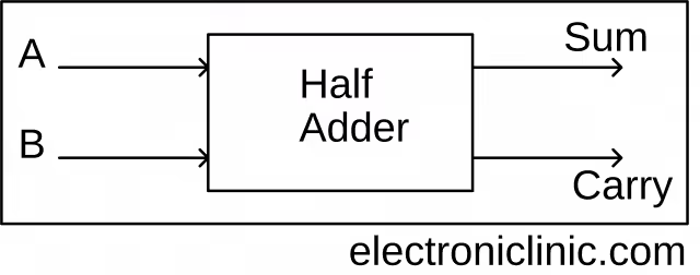
A combinational circuit that performs the addition of two bits is called a Half Adder. It receives two inputs and produces two outputs Sum and Carry. The block diagram for a half adder is as follows.
Designing of Half Adder:
Designing of Half Adder involves the following steps.
- Problem: addition of two bits.
- The number of available inputs are two.
- The input and output variables are assigned letter symbols. Let’s represent the inputs by A AND B, and the outputs SUM and Carry by S and C respectively.
- Truth Table
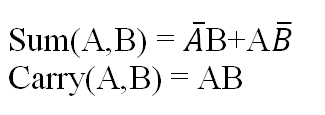
- Simplified Boolean function.
The Sum and Carry are in simplified form and further it cannot be simplified.
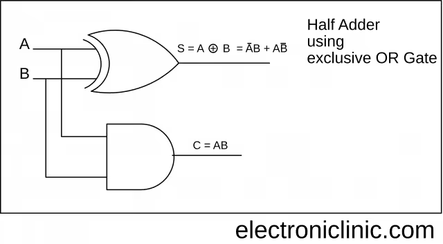
Half Adder Logical Diagram:
We can also obtain the logical diagram for Sum and Carry by using the Exclusive OR gate.
Full Adder:
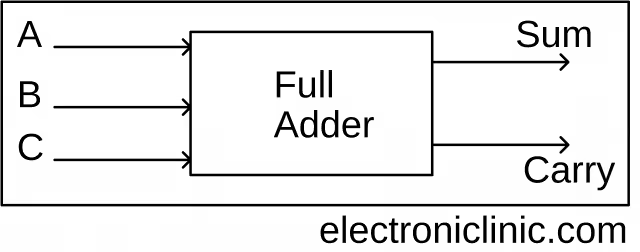
A combinational circuit that performs the addition of three bits is called a Full Adder. It receives three inputs and produces two outputs Sum and Carry. The Block diagram for the Full Adder is shown below.
Designing of Full Adder:
The designing of Full Adder involves the following steps.
- Problem: Addition of three Bits.
- The number of available inputs are three.
- The input and output variables are assigned letter symbols. Let we represent the inputs by A, B, and C; and the outputs by S and C i.e. S for Sum and C for Carry.
- Truth Table
- Simplified Boolean function.
Now let’s check if we can further simplify the Boolean functions of the Sum and Carry using the Karnaugh Map K Map.
The Boolean function for Sum cannot be further simplified.
Now, we will simply the Boolean function of the Carry using the Karnaugh Map K Map.
Carry = C = AC + AB + BC
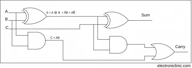
Full Adder Logical Diagram:
The logical Diagram for Sum can also be obtained by using the Exclusive OR Gate.
We can also design a Full Adder by using two Half Adders.
Full adder block diagram using two half adders
Logical Diagram of the Full Adder using two Half Adders:
Discover more from Electronic Clinic
Subscribe to get the latest posts sent to your email.






thanks for perfect adder knowledge ?