Buck Converter Designing and Working Explained
Last Updated on October 3, 2024 by Engr. Shahzada Fahad
Buck Converter:
Buck converter circuit works by reducing the voltage at the input. Now there are a lot of other circuits that can reduce the voltage such as a voltage divider circuit using two resistors or even Zener diodes and linear voltage regulators. You can use them to not only reduce the voltage but maintain a constant output voltage as well but those types of devices they reduce the voltage by dissipating power as heat. This circuit reduces the voltage not by dissipating power as heat but by stepping up the current.
We will be exploring the design process and working of a Buck converter which is used to lower the DC voltage efficiently. If you have a source, let say DC and a switch that is turned on and off periodically, you get a PWM signal. The amount of time a digital signal is in the active state relative to the period of the signal is called its duty cycle. Suppose that we leave the switch off all the time with the switch off 100% of the time, the output voltage will equal the voltage of the battery.
If the switch is on for a long duration, the duty cycle increases, and if it’s on for a short duration, the duty cycle decreases. Now, if you calculate the average of a cycle, with duty cycle 50 percent, it is half of the input voltage that is we have reduced the voltage from 12 volts to 6 volts with just a switch.
This converter can be used in circumstances where the required output voltage is lower than the input voltage the converter converts the voltage downwards the basic operation is as follows when the switch is closed current starts to flow through the components as indicated. If we assume that the output voltage of the buck converter is constant there is a constant voltage drop across the inductor as we know from elementary network theory a constant voltage drop across an inductor causes the current flowing through that inductor to rise linearly with time DLDT is constant and the proportionality factor is the inverse of the inductance value L of the component the linear increase of the current in the inductor is shown in a graph this operation phase of a converter where the first or primary switch is closed is called the primary stroke.
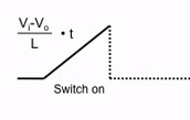
When the switch is turned off the current and the inductor keeps flowing but the only path that the current can take is through the diode which basically operates as the second switch in the power conversion. Network again there is a constant voltage across the inductor please notes that the sign of the voltage across the inductor was changed when the switch turned off and the diode turned on because of the new voltage across the inductor the current decreases linearly with time this is shown in the waveform graph.
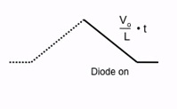
In the graph the rising and falling slope are shown as approximately the same but with different sign impractical circumstances. This is generally not the case but for the sake of clarity they are shown as such in this explanatory graph. The operation phase where the second or secondary switch is closed is called the secondary stroke the relation between the input voltage VI and the output voltage Vo is given in the first equation:
V0/Vi = δ
V0=δ Vi
Vswitch= Vi+ Vdiode
Vdiode= Vi

For efficiency reasons, we will replace it with an electrical switch, or a MOSFET. This MOSFET is controlled by a PWM signal. But this is just the amplified PWM signal and it has high voltage peaks. To smooth this we add an inductor in series with the load.
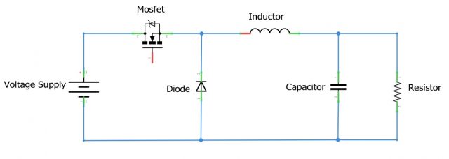
Suppose we control this gate voltage in a way such that the transistor behaves like a switch, which we can turn on or off. If we close the switch, we will cause a DC voltage to appear across the inductor. The current through the inductor will keep increasing, so long as the switch is closed. The current through an inductor cannot change instantaneously. Inductor wants to keep the current constant through itself and for that it will instantly change the voltage across itself. As the switch closes, the current starts to flow. To resist this flow, the inductor drops the voltage at another end to zero, creating equal and opposite voltage to the battery. This is possible due to the magnetic fields which are generated in the inductor. But it can’t resist it for a long time, thus the current starts flowing and voltage at the other end starts rising. Also, the inductor starts storing the energy in its magnetic fields. After some time the magnetic field stabilizes and the inductor will act as a closed switch, allowing maximum current to flow. Now, if you open the switch, then there is no source to supply current and thus current starts falling. But as you know current through the inductor cannot change instantly. Hence, now the inductor act as a battery supplying current but it slowly runs out of energy. As this end is open, the electrons accumulate here creating a high negative voltage.
This may damage the components. Thus we add a low voltage drop, Schottky diode to create a path for electrons. But the voltage at the load still has high voltage spikes. Hence, we increase the frequency of the PWM signal, such that the voltage and current by the inductor remains somewhat stable. This is also the reason why the switch mode power supply uses high frequencies. To further smooth-out them we add a capacitor in parallel. Capacitor wants to keep the potential difference constant across itself and for that it will change the current through it. As the switch closes, the voltage increases to 5 volts. To resist this, the capacitor flow current through itself, raising the other terminal to 5 volts.
This is possible due to the electric fields which are generated in the capacitor. But it can’t flow current for a long time as the plates get charged, thus the current reduces, and voltage at the other end starts dropping to the ground. Also, the capacitor starts storing the energy in its plates. After some time the plates get fully charged, thus no current can flow and the capacitor act as an open switch.
Now, if you open the switch, then there is no source to supply voltage and thus voltage starts falling. But as you know voltage across the capacitor cannot change instantly. Hence, now the capacitor acts as a battery supplying current. But it slowly runs out of energy and thus the flow of current reduces and after some time it stops, thus the voltage drops. We have created is the buck converter. But, there are some issues, as the load changes the voltage across the load also changes, so we need to create feedback to change the duty cycle of the PWM signal with respect to the load.
The voltage at the output is reduced by a voltage divider and it is fed into an op-amp which acts as an error amplifier. This component is known as an Operational amplifier or an Op-amp in short. It has two inputs and one output, the other two terminals are for the supply voltage. It is used to amplify the difference between the inputs. It compares both the input. If the voltage at the non-inverting input or the Positive terminal is greater than the inverting one, then the output is the positive supply voltage or, if the voltage at the inverting input or the Negative terminal is greater than the non-inverting one, then the output is the negative supply voltage.
In this configuration, the op-amp wants to keep both of its inputs at the same voltage and for that, it will change its output. As the feedback is to negative input, the output varies according to the voltage at the negative input. This can be seen as a see-saw. When the input voltage falls, the output rises. When the input rises, the output falls. This is how the differential amplifier works. This is a Triangle wave generator. The output of the error amplifier and wave generator is fed to another Op-Amp which acts as a comparator and outputs the PWM signal which controls the MOSFET. Here the negative input is a constant voltage from the differential amplifier, and the positive input is the wave form triangle wave generator. Hence, when the triangle wave is higher than the constant voltage the output is the positive supply voltage. Here it is plus five volts and when the constant voltage is higher than the triangle wave, the output is the negative supply voltage. Here it is ground or zero volts. This is how the comparator works.
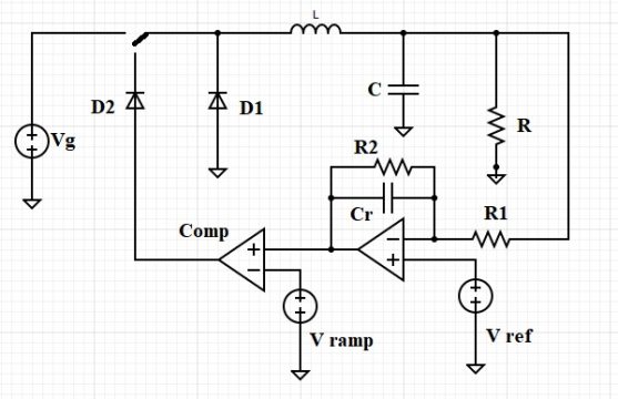
If the constant voltage increases, then the width of On-time decreases, and if the voltage decreases, the duty cycle of PWM also decreases. This is a P-channel MOSFET. An N-channel MOSFET will turn on when the gate voltage is above the source voltage, and a P-channel MOSFET will turn on when the gate voltage is below the source voltage. So when the PWM is high the MOSFET is off and when the PWM is low MOSFET is on. Hence, the duty cycle of PWM and MOSFET is the opposite as one increases other decreases. But you may think, why not use an N channel MOSFET, because, it is on when the gate is high, and off when the gate is low.
Because the voltage at the gate required to turn on the n-MOSFET should be higher than the source voltage, and during operation, the drain and source voltage will be almost the same. Thus we need higher than Vcc at the gate to turn on the MOSFET. Hence, we use a P-MOSFET also; we add a pull-up resistor between source and gate. This is the positive supply from the battery. These voltages are created with the help of voltage regulators. As these voltages are used only for references, thus there is no current drawn from them and no power is lost. In real cases, due to non-ideal components, some power is lost as they draw a small amount of current. Now, let’s look at the working of the complete circuit.
We will have an input voltage of 12 Volts, and we want the output of 5 Volts irrespective of the load. Now, If we increase the load, the current increases, but the PWM is the same as before, hence the voltage falls. This causes the voltage at the reference to fall and thus increasing the difference between this and reference at the differential amplifier. This increases the voltage at the output and then the duty cycle of PWM decreases from the comparator thus increasing the on-time of MOSFET and increasing the voltage at the load.
Also, we can change the voltage by changing the value of the potentiometer. This change in resistance will affect the feedback voltage, thus it will change the output of the error amplifier and then change the PWM signal. Now, while designing this some care should be taken. First, the voltage at the error amplifier should always be below this reference voltage. Hence, we select the feedback voltage divider such that the voltage does not exceed 2 volts. Thus the resistor value turns out to be 100 Kilo ohm and 20 k trimmer. But, this will reduce the voltage to a minimum of 6 volts. Hence, we use a 100-kilo ohm trimmer. For this arrangement of the op-amp and the value of the resistor, the minimum output voltage is nearly 4.5 volts.
For these values, If the load is reduced by a large amount, the reference voltage may rise above 2.5 volts as the energy storage components release their energy. This isn’t an issue with this analog circuit as the error amplifier will output zero volts and this will turn off the MOSFET. But, for a digital PWM controller, this may cause some problems or damage them. The second is the inputs of the comparator. In this arrangement, we get a range from 12 to 5 volts for this feedback resistor values and If the inputs of the comparator are reversed then the range becomes 8 to almost zero volts. Also, the high voltage output is towards the high end of the trimmer. This is how the closed-loop buck converter works. The voltage and current from the source are converted to lower voltage and higher current at the output.
Read my article on voltage doubler using a 555 Timer IC.
Discover more from Electronic Clinic
Subscribe to get the latest posts sent to your email.
