Complementary MOS or CMOS, CMOS as Analogue switch
Last Updated on May 23, 2022 by Engr. Shahzada Fahad
Table of Contents
Complementary MOS or CMOS:
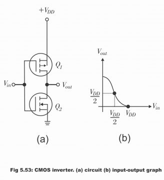
Complementary MOS or CMOS are such basic circuits in which two complementary or matching MOSFETs are used, which are properly arranged together in a series in such a way that if any one of these conducts (i.e. turns on), the other remains off during the period. In other words, CMOS is an integrated circuit, which consists of two complementary MOS (i.e. one P channel MOSFET and another N channel MOSFET). In case of a high or low input of such circuits, both these MOS conduct alternately. That’s both these devices (i.e. N channel and P channel MOSFET) are applied together in such a sequence on the circuit that when one of the diodes is ON, the other device remains OFF at that juncture. Both these devices are complementary i.e. their VGS (off), VGS (on), ID (on), and all other values are either mutually equal or opponent. In diagram 5.53 (a), a CMOS inverter circuit (a circuit that is used for switching purposes, is called an inverter circuit) has been shown, which consists of a P channel MOSFET (i.e. Q1) and an N channel MOSFET (i.e. Q2)
Figure 5.53 (a) CMOS Inverter Circuit (b) input-output graph
Basic Action
When the circuit displayed in diagram A is used for switching objectives, its input voltage (Vin) is either high (i.e. +VDS) or otherwise low (i.e. zero volts). When input voltages are high, the VGS value of the lower N channel MOSFET is higher as compared to its threshold value, due to which it turns on. In the meantime, the VGS value of P channel MOSFET located on the upper side, becomes zero, due to which it turns off (in other words, when input voltages are high, Q2 turns ON while Q1 powers OFF). In such a situation, output voltages of shorted Q2 (which is ON) gets lowers and get equal to the ground level (i.e. zero volts, because Q2 output has been fixed to the ground). This low output results in spite of high inputs. Thus, the circuit reacts like an inverter.
On the contrary, when input voltages are low, the VGS value of upper channel MOSFET exceeds its threshold value, as a result of which, it turns ON. Thus, a high voltage is accessible on the VDD terminal adjacent to Vout. However, it must be remembered that lower N channel MOSFET remains OFF during this period, because its VGS value is zero (in other words, when input voltages are low, Q1 powers ON whereas Q2 remains OFF). Under such a situation, high output voltages i.e. +VDD are accessible across the shorted Q1. As output voltages are inverted (i.e. as output voltages are precisely opposite to the input voltages applied on the circuit), therefore such type of circuit is called an inverter circuit.
In figure (b) it has been revealed through a graph how output voltages change as a result of the change in the input voltages. When input voltages are zero, output voltages are high. Conversely, when input voltages are high, output voltages are low or they tend to become zero. A point exists between these two extreme values where input voltage equals VDD/2. At this point, resistance and output voltages of both MOSFETs are equivalent i.e. (VDD/2).
As two MOSFETs are fitted in series on a CMOS circuit and as one of them always remains OFF, therefore only leakage current flows through the non-conducting or off the device, the value of which is usually extremely low (i.e. in nano amperes). As its resistance is measured in mega-ohms, therefore the greatest advantage of a MOSFET circuit is that they consume a very small amount of power. Due to its low power consumption quality, CMOS are commonly used in integrated circuits e.g. calculators, digital watches, mobile radios-cellular phones, hearing aids etc.
The CMOS Analogue Switch
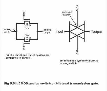
A CMOS analogue switch (which is also called a bilateral transmission gate) is manufactured by fixing an NMOS device across the PMOS device. Thus, this assembly behaves like two such parallel switches, which close or open together simultaneously. In fact, when switches are closed, both transmit or conduct positive and negative signals. However, one of them passes very large positive signals while the other one can pass very negative signals.
In figure 5.54 (a), both the devices are connected parallel while in figure (b) a CMOS switch symbol has been illustrated. It is evident from the figure that PMOS substrate terminal with an exceptionally +ive voltage (+VDD) and NMOS substrate with a very negative voltage (-VDD) are fixed together. In the figure, two inputs (C and C) have also been shown (remember that the inverse, inverse or complement of C is denoted by putting a small line above C, which is called a bar). Thus, if C is high, C is low and if C is low, C is high. Both these inputs are switch control inputs, which indicate whether an analogue signal has to be transmitted through an output or it is going to be blocked. For the purpose of control of the switch, we have just to modify the level of C, while the level of C becomes inverse to the level of AC automatically. In the symbol shown in figure (b), C input has been reflected by inserting a round circle or bubble on C, which indicates inverted input.
Figure 5.54– CMOS Analogue Switch or Bilateral Transmission Gate
Suppose +2V is supplied on NMOSFET VT and -2V on PMOSFET VT. Further, VSS =-5 and VDD=+5. Suppose that analogue input can be varied continuously between +5V and -5V and that either +5V or -5V is applied on C or C. when C is supplied -5V, the gate of NMOSFET is at -5V and thus it remains OFF for all input voltages within the range -5V to +5V (it needs to be above -7V turning it ON). As there is +5V on C, therefore PMOSFET gate is on +5V (i.e. +5V are present on a gate and it also remains OFF between the range -5V and +5Vfor all input voltages (for turning it ON, its input requires to be greater than +7V). Thus, the analogue switch remains ON while supplying -5V on C.
Now assume that the value of C is +5V. in such a situation, there is +5V on the NMOSFET gate and it remains ON due to the input voltages received within the range -5V to +3V. As there is -5V on C, (i.e. C=-5V) therefore, PMOSFET remains ON for input voltages within the range +5V to -3V. A conducting path from input to output for all input voltages within a range of +5V to -5V exists between these two devices and we can conclude that under C=+5V analogue switch remains closed. In figure 5.55, the conductive input voltages of all the devices have been shown. It is also apparent from the diagram that both devices conduct within the input range +3V and -3V.
Figure 5.5 – The range of analogue input voltages over which a MOSFET conducts when the CMOS analogue switch is ON (C=+5V). Note that both devices conduct in the range from -3V to +3V. NMOS Vi= +2V : PMOS Vi=-2V)
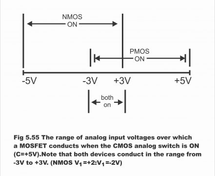
The range of analogue input voltages over which a MOSFET conducts when the CMOS analogue switch is on (C=+5V). Note that both devices conduct in the range from -3V to +3V (NMOS Vi=+2; PMOS Vi=-2V)
Previous Topic: MOSFET as a Switch
Next Topic: Thyristors
For electronics and programming related projects visit my YouTube channel.
Discover more from Electronic Clinic
Subscribe to get the latest posts sent to your email.
