Types of Random Access Memory or RAM in Digital Electronics
Last Updated on March 23, 2023 by Engr. Shahzada Fahad
Table of Contents
Random Access Memory or RAM
A type of semi-conductor memory, in which stored data can be read when required and that data can also be modified, stored or read and write according to one’s needs, is called Random Access Memory (RAM). As the contents of this memory or the stored data on it, can be read and new contents or data can also be written on it, therefore this memory is also called read/ write memory. It is a volatile type of memory, which means that as soon as power supply turns off, data stored on a RAM is lost or wiped out. The major share of memory in personal computers consists of RAM, wherein typed data or and programs are stored or saved with the help of keyboard. If the typed data has not been saved, then entire data wipes out or erases as soon as power supply turns off (i.e. it is a temporary kind of memory as unsaved data is lost as soon as supply powers off). As such RAMs are used in places where there is a need for temporary memory. For example, calculators, memories, buffer memories and microcomputer memories etc.
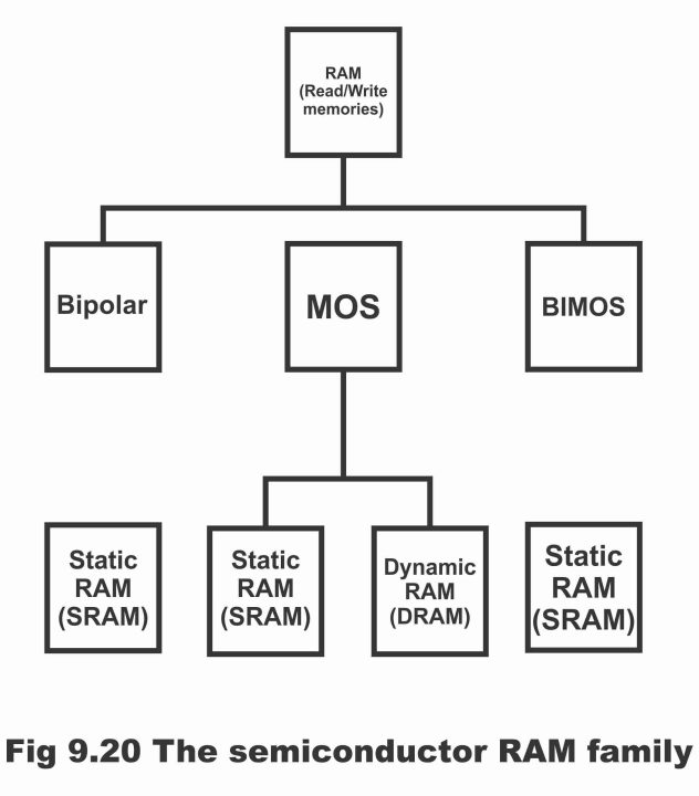
Semi-conductor RAM can be manufactured by means of either bipolar technology (i.e. TTL, ECL or Short Key TTL) or MOS technology. However, some of the memory devices can be manufactured through a combination of both bipolar as well as MOS technology. Such types of devices are called BiMOS. All bipolar RAMs are static RAMs (or SRAMs) which are fabricated via flip – flops or latches and data stored on it can be protected for a very long period of time, provided power remains on. The access time (time required for reading some stored content or word on any memory location after application of address bits, is called access time) of bipolar flip – flops is about 35ns and a package contains approx. 1K cells. Some MOS RAMs are of static type and some of dynamic type. A dynamic RAM (DRAM) memory is a memory, where in data is being stored inside capacitor, which requires a re- charge from time to time in order to keep the data protected. Access time of MOS devices is about 400ns, however they are quite bulky in size. Remember that RAM can either be of static or dynamic type. In figure 9.20, RAM family has been illustrated.
Figure 9.20 – The semi–conductor RAM family
Static RAM
RAMs which are manufactured via application of bipolar or MOSFET flip – flop application, are called static RAM (SRAM). These RAMs are of volatile type and if power does not turn off, data can remain stored within it for a long period of time. Moreover, stored data does not require a refresh or recharge from time to time. In order to read or write data in a static RAM, only address and control bits are supplied.
In figure 9.21, logic diagram of static RAM cell has been illustrated, the operational process of which is as below;
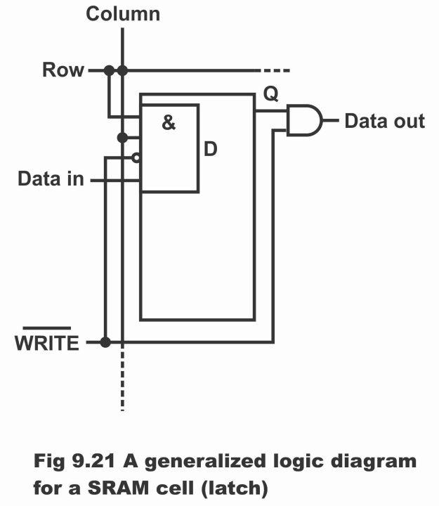
This cell (or group of cells) is selected by means of rendering rows and columns lines high. When WRITE line is low (i.e. on write) then input data bit is stored or written on cell in such a manner that on a set cell (which is generally D type flip – flop) 1 stores on it and reset of cell, 0 stores on the cell. When WRITE line is high (i.e. on read), no impact occurs on cell, however stored data bit (Q) will shift towards data output line.
Address system of a static RAM is just similar to a ROM with the only exception that read/write control also exists in SRAMs apart from data inputs. In order to specify the organization of a SRAM, 32K x 8bit memory is used. The logic symbol of this type of memory has been illustrated in figure 9.22.
Figure 9.22 – logic diagram for a 32 x 8 SRAM
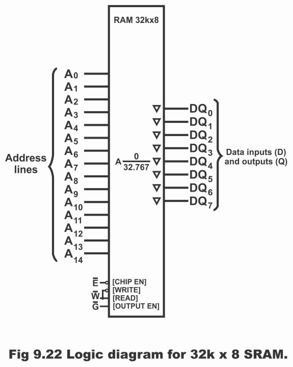
In READ mode, 8 data bits which are stored on selected address, are reflected on data output lines. In WRITE mode, 8 data bits, which are provided on data input lines, are stored on the selected address. Data input and data output lines (DQ0 to DQ7) are same lines. During READ operation, these lines behave similar to input lines (Q0 to Q7) and in WRITE operation, these lines function as input lines (D0 to D7). Static RAMs (SRAMs) can be organized in a specific range up to 4MB (or 4 mega bytes) with a capacity of single bits, nibble (4- bits), byte (8 – bits) or multiple bytes (16, 24 or 32 etc.). In figure 9.23, basic organization of a peculiar 32K x 8 SRAM has been displayed. The memory array shown in this figure contains 256 rows and 128 x 8 columns (every column out of which comprises 4 – bits). In fact, there are 1215 = 32,768 addresses in this figure and each address consists of 8 – bits. The capacity of this type of memory is 32,768 bytes (i.e. 32 kilo bytes) or 262,144 bits. Eight out of the 15 address lines shown in the figure are being decoded via a ROW decoder, so that selection of any one particular row (out of 256 rows) could be made. Whereas, remaining seven address lines out of 15, are being decoded via a column decoder, so that any one column out of 128 x 8 bits columns could be selected.
Figure 9.23 – Basic organization of a 32 x 8 SRAM
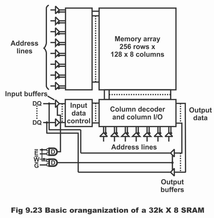
First of all, chip is enabled or activated, under which low level is applied on E in order to operate the memory. In other words, E is retained low.
In READ mode (i.e. when data is required to be read on any memory location), write enabled input W is turned high or deactivated and output enabled G, is done low active. As such, input buffers, disable via gate G1 (i.e. stop working) and column output enable (i.e. start operating) via tri – set (having three conditions) buffers (a circuit which protects input and output from loading, is called buffer) gate G2. Thus, 8 data bits of the selected address shift towards data lines (D0 to D7) via I/O.
In WRITE mode (i.e. when some data is required to be written or stored in memory), W is activated (or low) and G is deactivated (high). As such 8 input data bits present on the input lines, pass through via input data control and store on the selected address via column I/O.
In figure 9.24, block diagram of a static RAM has been illustrated, which is also frequently used to explain SRAMs operation. According to figure, such memories are mostly fabricated along “n” address lines, which during its operation selects just one 2n cell at a time from the entire cells found on a memory array (i.e. one bit is selected at one time). In this memory, a chip enabled control (CE), a write enabled control (WE), a single input data bit (D1) and a single output data bit (D0) are also being organized or arranged. Operational mechanism of this type of static RAM has been illustrated in figure 9.25.
Figure 9.24 – Generalized block diagram for a static RAM
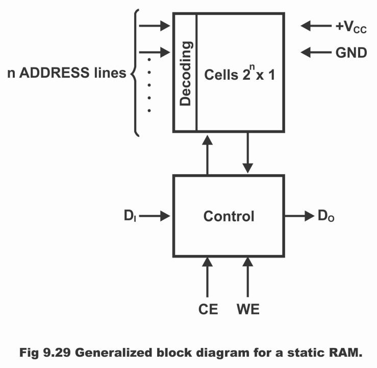
First, selection of a memory location is done by means of address lines. The write or read or hold operation is selected by means of control signals WE and CE (as this memory has total three positions write, read and hold, therefore it is a tri – set or a three-set memory, which is most profusely used). Here, WE mean write – enabled signal and CE means chip – enabled signal.
Figure 9.25 – Table for Static RAM
| CE | WE | Operation | Output |
| 1
1 0 |
1
0 x |
Write
Read Hold |
Floating
Connected Floating |
Write operation occurs when both CE and WE are high, which means that input data has been stored on addressed memory location and during this operation, three state output data lines are in a floating state. When CE is high and WE are low, then read operation takes place, as a result entire contents of addressed memory locations appear on data output lines, because the internal three state switches are closed at that time.
When CE is low, such a state is called holding. No operation takes place during such a state and entire data available on different memory locations, remains unchanged. However, under such a condition, output data lines tend to be in a floating state, as has been depicted via table.
In figure 9.26, a MOS static RAM cell (which is a flip–flop) or a memory element has been illustrated, wherein both transistors Q1 and Q2, operate as switches. Whereas Q3 and Q4 transistors, act as active loads or resistors. Remember that when Q1 conducts, Q2 remains off at that time and when Q2 conducts, Q1 remains off at that time. A static RAM comprises thousands of such flip – flops, wherein every flip–flop stores a bit. Flip–flop remains in a latched state as long as power is on and it stores bit (0 or 1) on its memory for an indefinite period of time.
Figure 9.26 – Static cell
In figure 9.27, a static bipolar RAM circuit has been illustrated. The circuit shown in figure 9.26 and this particular circuit, both operate in a similar fashion (static RAM are either MOS type or bipolar type from manufacturing point of view) elaboration of which is as follows;
According to the circuit displayed in figure (a), collector of every transistor is connected with base of the opponent transistor via a resistor (i.e. collector of every transistor drives base of the opposite transistor via a resistor). In this type of circuit, when one transistor saturates or turn on, the other transistor remains off at that time. for example, if right end transistor saturates, its collector voltages almost become zero. It means that zero voltage are received on the base of left end transistor, as a result it cuts off (i.e. it does not operate). However, its collector voltage rises to +5V. As a result of these high voltages, a huge base current generates in the right-side transistor, which helps it to sustain on a saturation state. Thus, overall circuit remains in a latched state, by means of which left – end transistor remains on a cut – off state, whereas the right – end transistor remains on saturated state. Resultantly, Q value is almost 0V and in this case, binary 0 stores in the circuit (because Q = 0)
Similarly, if the left–end transistor saturates, in such a situation right – end transistor cuts – off, as has been shown in the figure. In this condition, Q value equals to approx.5V. Thus, binary 1 store on circuit, in such a case (because Q = 1).
Figure 9.27 – (a). latched state (b). alternative state (c). trigger inputs
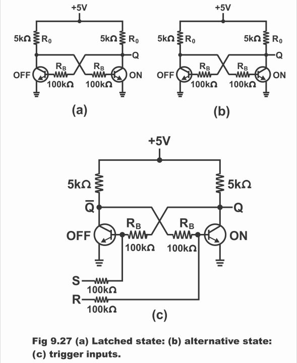
Inputs can be included in order to control stored bits in a latch or flip – flop or memory cell as illustrated via figure ©. These control inputs are low (i.e. 0) or high (i.e. +5V). When input S rises, left – side transistor saturates. As soon as left – end transistor saturates, a latch state develops on the circuit as a whole and q value becomes 1. Once Q value becomes 1 (i.e. when circuit in a set state) then so long as input S value does not return to 0V, remains stable on its state i.e. Q =1 (this process is called latching).
When a high reset input is provided on input R, then right – end transistor saturates. As soon as this happens, circuit latches on Q = 0 state (i.e. reaches on Q = 0 state and its state does not change until R input turns low once again). In the figure ©, Q refers to the stored bit whereas complementary output received from the left – end transistor tends to be Q. As Q depends on its use or application, therefore it is sometimes used and sometimes not applied.
Dynamic RAM or DRAM
Dynamic RAM (DRAM) is a type of memory in which data is stored within capacitors and for the purpose of protecting the stored data, capacitors are recharged periodically (because memory elements or memory cells in this type of memory are capacitors instead of flip – flops, which gradually discharge as a result of leakage). The greatest drawback of this type of memory is its frequent recharging requirements, because in case it is not recharged, data stored on it gets wiped out or lost completely after some time. As just two components are required for designing a dynamic RAM (i.e. MOSFET and capacitor) therefore, a DRAM consists of more memory cells as compared to a SRAM, owing to which it is being generally preferred. In other words, a dynamic RAM can store more memory locations as compared to same – physical sized and same – area specific static RAM and its price per bit also turns out to be low. It ought to be remembered that a dynamic memory cell consists of a MOS transistor circuit and a storage capacitor whereas a DRAM is composed of thousands of such memory cells. However, one of a demerits of the dynamic RAM is that its capacitor requires to be refreshed or recharged intermittently after every few milli seconds. As a consequence of this flaw, its design is somewhat complicated (because it requires more circuitry). In short, working with a static RAM is easy comparatively to a dynamic RAM.
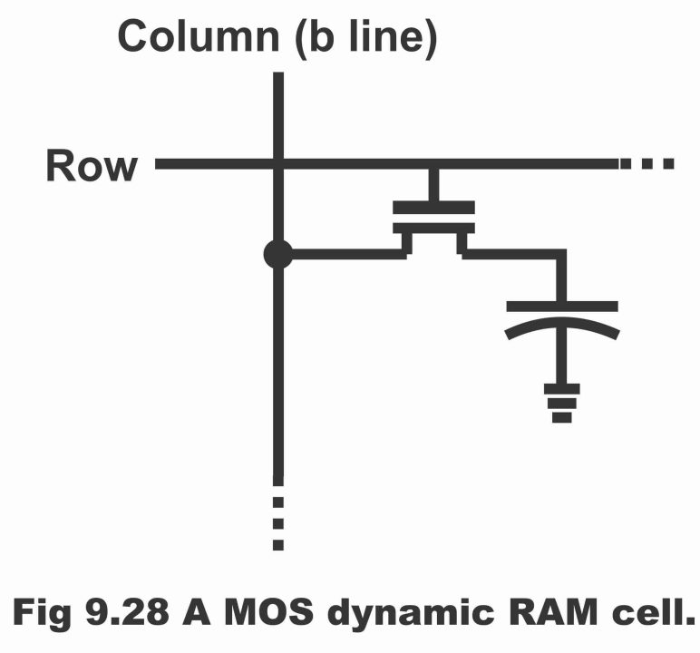
In figure 9.28, a dynamic RAM cell has been portrayed, which contains one MOS transistor and one capacitor. In this cell, transistor operates as a switch. For simplicity purposes, its operation has been depicted via figure 9.29 (a) as follows;
Figure 9.28 – A MOS dynamic RAM cell
When W line (WRITE mode) is low, in such a situation, tri- state or tri – state input buffer enables (i.e. start to operate) whereas output buffer disables (i.e. stops to operate). In order to write or store 1 on cell, both DIN and row lines must essentially be high, so that transistor could remain on. When both DIN and row lines are high, transistor operates as a closed switch in order to connect capacitor with the bit line. As a result of this process, capacitor starts to charge until the positive voltage. This has been reflected via figure (a).
Figure 9.29 – basic operation of a DRAM cell
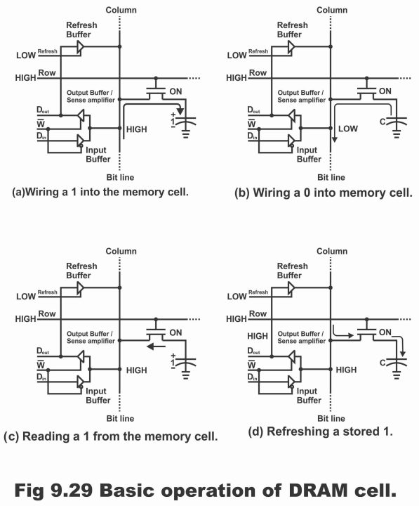
When 0 is desired to be stored, DIN line is turned low. As such, no charge deposits during storing process of the capacitor 0 (i.e. during 0 storage operation, no charge occurs on the capacitor). However, when it has been storing 1, it tends to discharge as illustrated via figure (b). When Row line is dropped low again, transistor turns off and capacitor also disconnects from the bit line. However, a charge (0 or 1) exists on the capacitor.
In order to read data existing on the cell, line W is turned high, due to which output buffer gets enabled (i.e. starts working), whereas input buffer gets disabled (i.e. stops working). When row line is turned high, transistor turns on and capacitor connects to the bit line. As such, output buffer (sense amplifier) connects with capacitor via bit line (i.e. start working). As a result, data bit appears on data output line (DOUT). This operation has been illustrated via figure ©.
For refreshing the memory cells, W line, row line and refresh lines are kept high. Thus, transistor turns on and connects capacitor on bit line. In such a case, output buffer enables (starts working) and stored data bit is applied on refreshed buffer’s input, which enables by means of a high refresh input. Thus, voltages are produced on bit line according to the stored bits and capacitor is re- filled via charging (i.e. it refreshes), as has been illustrated via figure (d).
Capacity of a RAM
The capacity of a static RAM as well as a dynamic RAM can also be expressed in the form of code numbers, e.g.
74189 = 16 x 4
2114 = IK x 4
6116 = 2K x 4
6264 = 8K x 8 … etc.
In the code number 74189 mentioned above, 74 represents TTL series, where as 189 in this number denotes name of RAM’s IC, while 16 x 4 means that this RAM consists a total of 16 memory locations (addresses) and four data lines. Therefore, total capacity of the RAM becomes 16 x 4 = bits (i.e. 64 bits can be saved on this RAM)
Total Capacity = Memory locations x Data lines
Similarly, according to RAM list mentioned above, 2114 code number memory consists of 1 kilo (1024) memory locations and 4 data lines. Here 21 means series number, 1 means 1 kilo memory locations whereas 4 refers to the number of lines. Thus, total capacity of this memory is as follows;
Total Capacity = 1024 x 4 = 4096 bits
74149 and 2114 code numbers memories static RAM memories. As these memories consist of 4 data bit lines, therefore they are used very rarely. Now-a-days, 8 – data lines memories e.g. 6116 and 6224 are most frequently used. The first two digits on the left of such memories reflect series number of these memories where as the remaining 2 numbers denote its capacity. For example, in 6116 code number RAM, 61 is series number of this RAM whereas 16 represents its capacity. As this capacity has been expressed in the form of bits, therefore if 16 is divided by 8, the capacity of this memory converts to bytes. i.e.
16 / 8 = 2K bytes
Here 8 represent data lines. Thus, total capacity of the RAM is as under;
Total Capacity = 2K x 8 = 2048 x 8 = 16,384 bits
Previous Topic: Erasable Programmable Read-Only Memory (EPROM) in Digital Electronics
Next Topic: Digital to Analogue & Analogue to Digital Converters
Discover more from Electronic Clinic
Subscribe to get the latest posts sent to your email.